High voltage switch circuit for semiconductor device

a high-voltage switch and semiconductor technology, applied in the direction of electronic switching, pulse technique, instruments, etc., can solve problems such as device disadvantag

Active Publication Date: 2007-01-02
SK HYNIX INC +1
View PDF3 Cites 14 Cited by
  • Summary
  • Abstract
  • Description
  • Claims
  • Application Information

AI Technical Summary

Problems solved by technology

Further, relative to a higher frequency operation in a semiconductor device, such a discharging time for the bias voltage increases to cause a disadvantage for the device.

Method used


Image

  • High voltage switch circuit for semiconductor device
  • High voltage switch circuit for semiconductor device

Examples


Embodiment Construction

[0012]Preferred embodiments of the present invention will be described below in more detail with reference to the accompanying drawings. The present invention may, however, be embodied in different forms and should not be constructed as limited to the embodiments set forth herein. Rather, these embodiments are provided so that this disclosure will be thorough and complete, and will fully convey the scope of the invention to those skilled in the art. Like numerals refer to like elements throughout the specification.

[0013]Hereinafter, it will be described about an exemplary embodiment of the present invention in conjunction with the accompanying drawings.

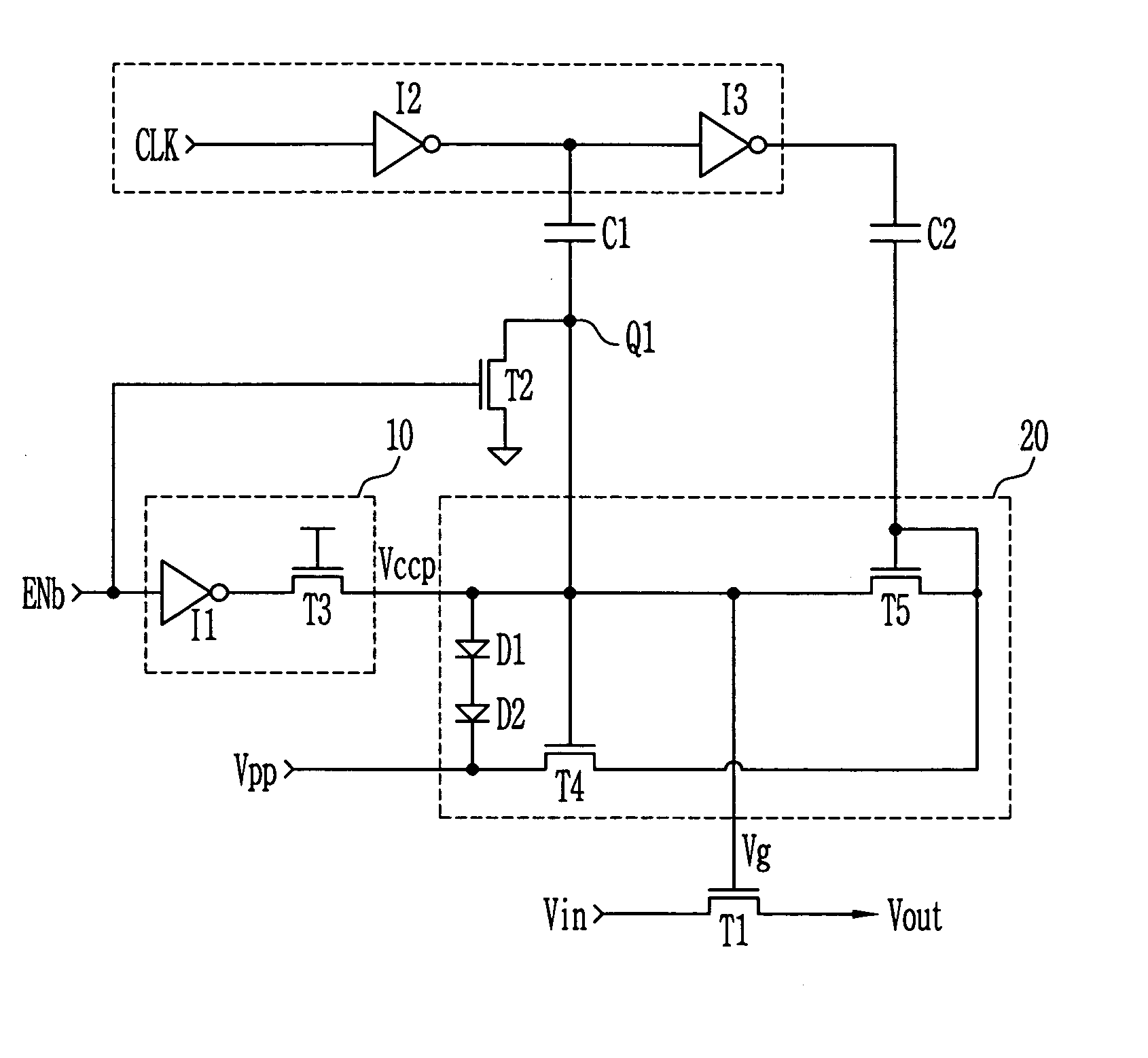
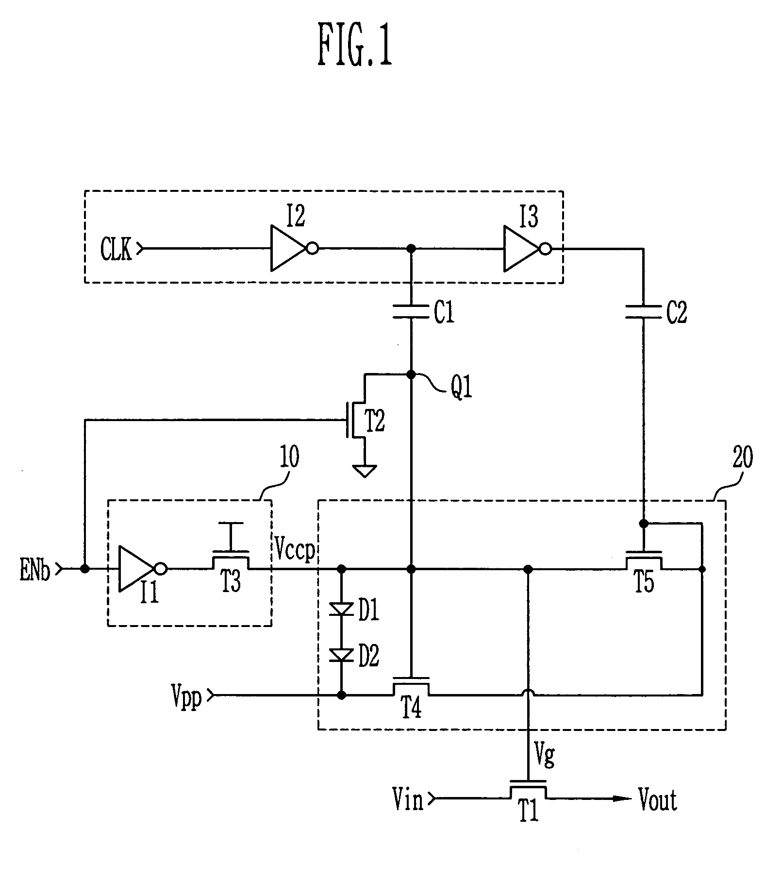
[0014]FIG. 1 is a circuit diagram of a high voltage switch circuit for a semiconductor device in accordance with the present invention.

[0015]Referring to FIG. 1, the high voltage switch circuit is comprised of a control node Q1 from which a control voltage Vg is generated, a first transistor T1 transferring a first high voltage Vin in...


PUM


Abstract

Provided is concerned with a high voltage switch circuit for a semiconductor device, which rapidly discharges a gate voltage of a pass transistor through an additional discharge transistor during inactivation of itself in the circuit structure with a positive feedback loop for transferring an internal high voltage without a voltage drop by applying an enough voltage to the gate of the pass transistor. The high voltage switch circuit prevents the internal high voltage from decreasing.

Description

BACKGROUND[0001]1. Field of the Invention[0002]The present invention is related to a high voltage switch circuit of a semiconductor device and particularly, to a high voltage switches circuit capable of rapidly discharging a high voltage.[0003]2. Discussion of Related Art[0004]A semiconductor device needs a high voltage pumped over an input power supply voltage, in which a high voltage transfer switch is required to pass the high voltage. In a conventional NAND flash memory, a pumping bias voltage is transferred to a wordline as a target voltage during a program operation or a read operation, for which a gate bias is boosted up from a floating state with a coupling level at a junction of a pass transistor by applying a bias voltage to the junction of the pass transistor at a time and thereby the wordline is charged with the bias voltage without a voltage drop.[0005]However, after transferring the target bias voltage, the gate voltage of the pass transistor gradually decreases for di...

Claims


Application Information

Patent Timeline
Patent Type & Authority Patents(United States)
IPC IPC(8): H03K17/16G11C16/06G11C16/12H03K5/153H03K17/06H03K17/687
CPCH03K17/063G11C16/12
Inventor KIM, DOE COOK
Owner SK HYNIX INC
Why Eureka
Try Eureka