Driving method of liquid crystal display panel and liquid crystal display device

a technology of liquid crystal display panel and driving method, which is applied in the direction of instruments, computing, electric digital data processing, etc., can solve the problems of limiting the thickness, weight and volume of the case, increasing the power consumption of the liquid crystal display device, and limiting the battery capacity

Inactive Publication Date: 2007-01-09
CITIZEN WATCH CO LTD
View PDF14 Cites 8 Cited by
  • Summary
  • Abstract
  • Description
  • Claims
  • Application Information

AI Technical Summary

Benefits of technology

[0025]Further, it is preferable that a voltage amplitude of at least one of the selection signal and the data signal is decreased as the selection period for selecting one scanning electrode by the selection signal is increased.
[0030]In this case, it is preferable that the selection period for selecting one scanning electrode by the selection signal is made shorter and a potential difference between the selection signal to be applied to the scanning electrode and the data signal to be applied to the data electrode is made larger when the amount of power generated by the power generating element or the amount of power stored in the storage battery is large than when it is small.
[0031]Further, the plurality of selection signals are switched at a set point of time, and one selection signal of the plurality of selection signals has a period during which a potential thereof to the data signal is positive and a period during which the potential is negative in the selection period of one scanning electrode, which makes it possible to prevent unbalance of charge in the liquid crystal layer by using the selection signal to eliminate the necessity for providing the refresh period.
[0041]It is preferable to provide the liquid crystal display panel drive circuit with means for making a potential difference between the selection signal and the data signal larger when the selection period by the selection signal is short than when the selection period is long, and to provide an operation member (selection button) for causing, from outside, the liquid crystal display panel drive circuit to select the selection signal having a different selection period.
[0042]In a liquid crystal display device provided with a power generating element, it is preferable to provide the liquid crystal display panel drive circuit with means for making a potential difference between the selection signal and the data signal larger when the selection period by the selection signal is short than when the selection period is long as well as for making the potential difference smaller when an amount of power generated by the power generating element is small than when the amount of power generation is large, and to provide an operation member (power-saving mode switching button) for forcing, from outside, the liquid crystal display panel drive circuit to increase the selection period by the selection signal and to decrease the potential difference.

Problems solved by technology

The output voltage and the output frequency of a circuit for applying a predetermined selection signal and data signal to the liquid crystal display panel accordingly become higher to increase the power consumption of the liquid crystal display device.
When the liquid crystal display panel is used for a small portable electronic device, however, there is a limit in thickness, weight, and volume of the case thereof and there is also a restriction in battery capacity.
Further, a liquid crystal display device having a power generating function is scarcely commercialized in the status quo.

Method used


Image

  • Driving method of liquid crystal display panel and liquid crystal display device
  • Driving method of liquid crystal display panel and liquid crystal display device
  • Driving method of liquid crystal display panel and liquid crystal display device

Examples


first embodiment

2

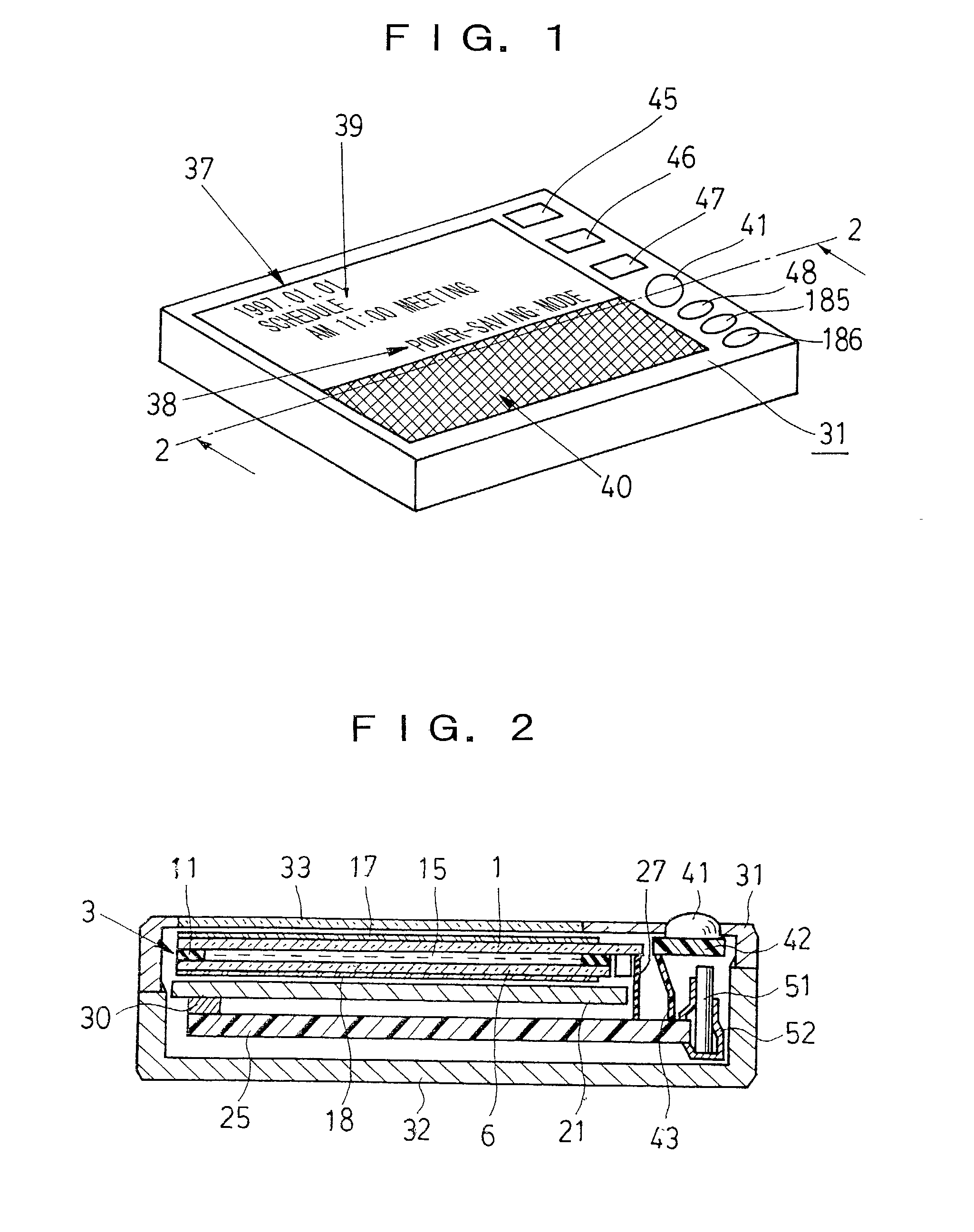
[0089]First of all, a configuration of a first embodiment of a liquid crystal display device according to the invention is explained using FIG. 1 to FIG. 4.

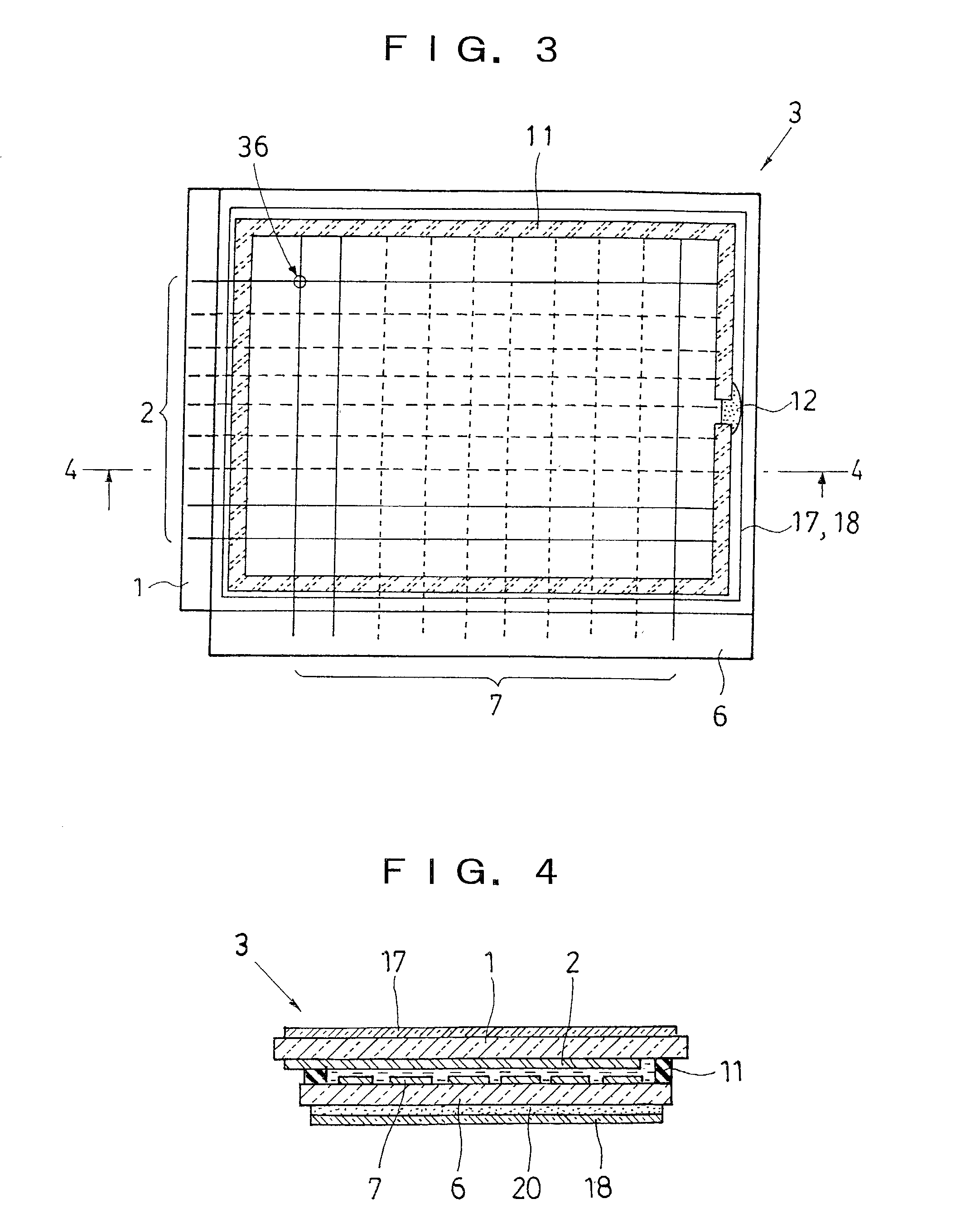
[0090]FIG. 1 is a perspective view showing an external appearance of the liquid crystal display device, FIG. 2 is a schematic cross-sectional view taken along a line 2—2 in FIG. 1, FIG. 3 is a plan view of a liquid crystal display panel provided in the liquid crystal display device, and FIG. 4 is a schematic cross-sectional view taken along a line 4—4 in FIG. 3.

[0091]The liquid crystal display device shown in FIG. 1 is a device which performs display in a display region 37 by the liquid crystal display panel and includes a power supply switch button 41, a scroll (+) button 45, a scroll (−) button 46, a mode switching button 47, a speaker 48, a display refresh button 185, and an electric power-saving (hereinafter, referred to as “power-saving”) mode switching button 186 to change the display or as input and output devices.

[0092]F...

second embodiment

14

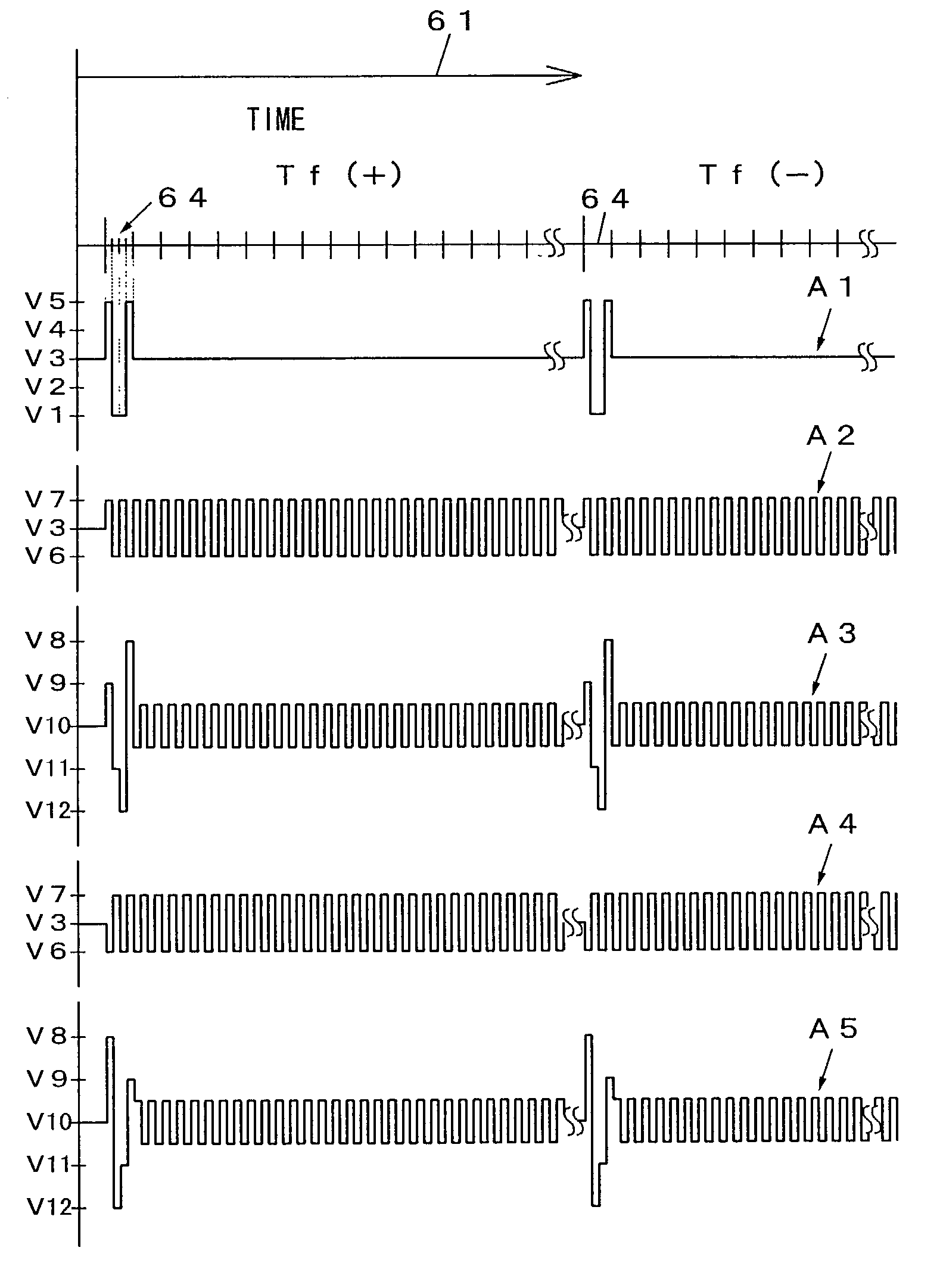
[0175]The driving waveform of a liquid crystal display device in the second embodiment of the invention is explained next using FIG. 13 and FIG. 14. The liquid crystal display device to which the driving waveform in this embodiment is applied is the same as that explained in the first embodiment using FIG. 1 to FIG. 6, and thus the explanation thereof is omitted.

[0176]FIG. 13 shows a second standard selection signal D1 and second standard data signals D2 and D3, which are the driving waveform in the standard mode in this embodiment.

[0177]FIG. 13 is also the same as FIG. 9 in that the horizontal axis is a time axis 61, the vertical axis represents voltage, and the middle of the scale set for each waveform shows a voltage of 0 V.

[0178]Each standard signal of the second embodiment of this invention applies an alternate current waveform by switching between signals of positive polarity and negative polarity for each field of Tf(+) and Tf(−). A voltage of positive polarity is applied i...

third embodiment

[0196]The driving waveform of a liquid crystal display device in the third embodiment of this invention is explained next using FIG. 15.

[0197]The liquid crystal display device to which the driving waveform in this embodiment is applied is the same as that explained in the first embodiment using FIG. 1 to FIG. 6, and thus the explanation thereof is omitted. Further, the driving waveforms in the standard mode explained in the first and second embodiments may be used for the driving waveform in the standard mode in this embodiment, and thus the explanation thereof is also omitted.

[0198]FIG. 15 shows a fourth power-saving selection signal F1 and a fourth power-saving data signal F2 which are the driving waveforms in the power saving mode in this embodiment.

[0199]FIG. 15 is also the same as FIG. 9 in that the horizontal axis is a time axis 61, the vertical axis represents voltage, and the middle of the scale set for each waveform shows a voltage of 0 V. However, write periods in a Tj(+) ...


PUM


Abstract

This invention is a driving method of a liquid crystal display panel in which a liquid crystal layer is sealed between a transparent first substrate formed with a plurality of scanning electrodes and a transparent second substrate formed with a plurality of data electrodes, the electrodes being formed on respective inner faces opposing each other, and portions where the scanning electrodes and data electrodes oppose each other with the liquid crystal layer sandwiched therebetween constitute pixel portions respectively, and which performs display by an electrooptical change having a memory property in the liquid crystal layer at each pixel portion, in which selection signals are applied to the plurality of scanning electrodes and a data signal is applied to the data electrode in correspondence with the selection signal of each scanning electrode to control the individual pixel portion independently, and a plurality of selection signals having different selection periods each for selecting one scanning electrode are selectively applied as the selection signals.

Description

TECHNICAL FIELD[0001]The present invention relates to a driving method of a liquid crystal display panel which enables a reduction in power consumption by driving a liquid crystal display panel, which performs display by changing optical characteristics thereof by applying voltage to a liquid crystal layer composed of a memory liquid crystal, at a low voltage or by stopping the driving signal in accordance with a driving environment, and a liquid crystal display device whose liquid crystal display panel is driven by the driving method.BACKGROUND TECHNOLOGY[0002]A liquid crystal display device is composed of a liquid crystal display panel and a drive circuit thereof, and the basic configuration of the liquid crystal display panel is such that a first substrate formed with many scanning electrodes on the inner face and a second substrate formed with many data electrodes, in such a manner to be perpendicular to the scanning electrodes, on the inner face, are bonded together with a fixe...

Claims


Application Information

Patent Timeline
Patent Type & Authority Patents(United States)
IPC IPC(8): G09G3/36
CPCG09G3/3629G09G3/3633G09G3/3651G09G2330/021G09G2300/0895G09G2310/06G09G2300/0876
Inventor SEKIGUCHI, KANETAKA
Owner CITIZEN WATCH CO LTD
Why Eureka
Try Eureka