
Liquid crystal display element driving method and liquid crystal display using the same

Inactive Publication Date: 2007-01-09
JAPAN DISPLAY CENT INC
View PDF9 Cites 8 Cited by
  • Summary
  • Abstract
  • Description
  • Claims
  • Application Information

AI Technical Summary

Benefits of technology

[0010]A second object of the invention is to provide a liquid crystal display element driving method and a liquid crystal display device using the method which enable a picture signal to be written to a pixel with reliability in the case of high resolution display.
[0034]With such constitution, the liquid crystal element is driven with a simple constitution.

Problems solved by technology

It is possible to achieve such bend orientation by transitioning an initial orientation which is called splay orientation through an application of a voltage; however, the bend orientation undesirably returns to the splay orientation when the voltage applied to the liquid crystals is below a predetermined value.
Therefore, the writing of the picture signal 101 causes a great potential difference, and the potential of the pixel electrode does not reach the potential responsive to the picture signal 101 to lead to generation of the display unevenness.
Further, along with future developments in high resolution liquid crystal panels, time allowed for writing one source signal will become shorter and shorter, and, therefore, it will be necessary to write a signal with reliability in such shortened period of time.

Method used


Image

  • Liquid crystal display element driving method and liquid crystal display using the same
  • Liquid crystal display element driving method and liquid crystal display using the same
  • Liquid crystal display element driving method and liquid crystal display using the same

Examples


first embodiment

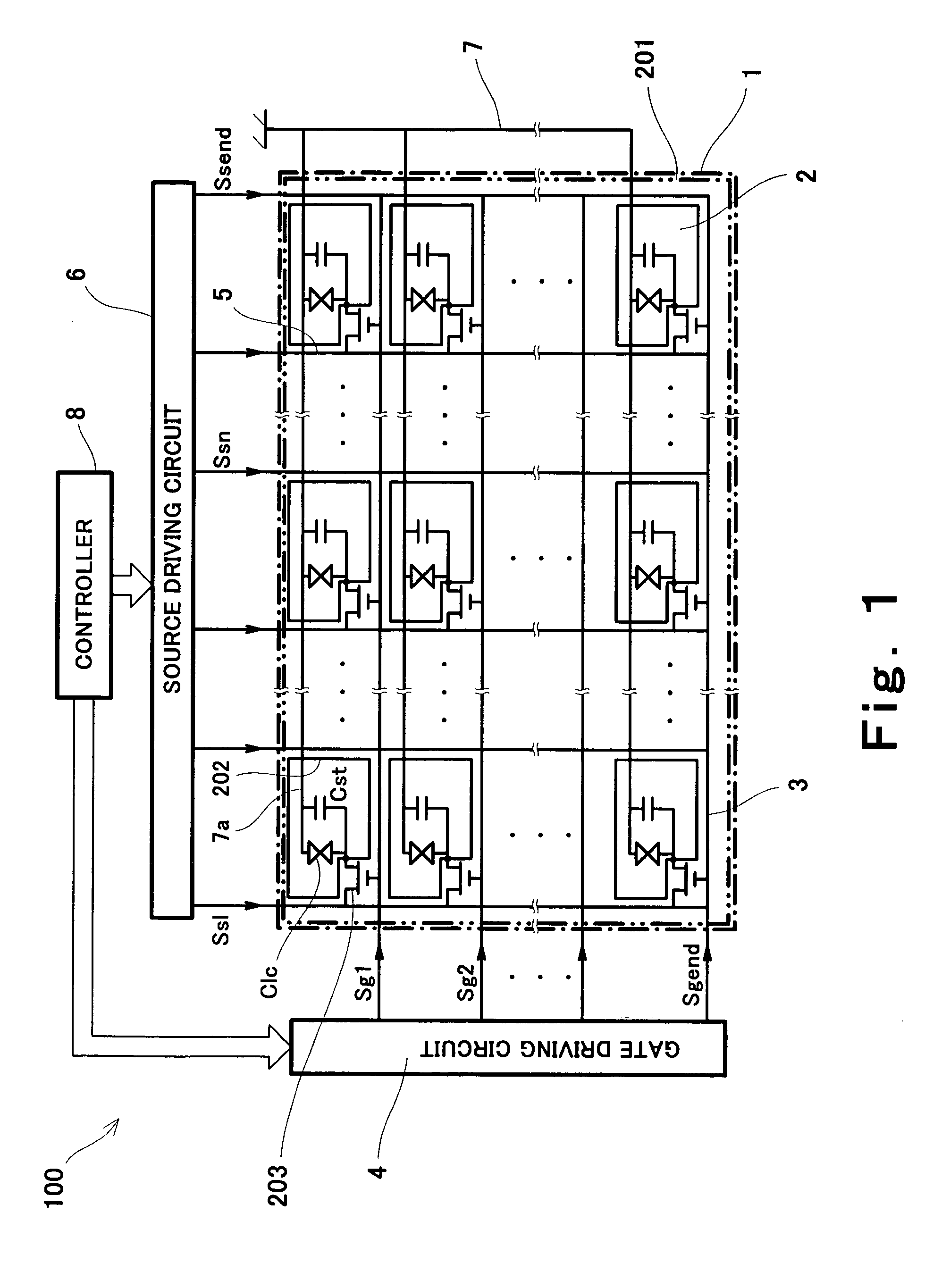
[0050]FIG. 1 is a block diagram showing an overall structure of a control system of a liquid crystal display device according to the first embodiment of the present invention.

[0051]As shown in FIG. 1, a liquid crystal display device 100 includes a liquid crystal display element 1, a gate driving circuit 4, and a source driving circuit 6, and a controller 8.

[0052]The liquid crystal element 1 is a known one, and it is of the active matrix type in this embodiment. The liquid crystal display element 1 has a TFT substrate (not shown), a counter substrate (not shown) opposed to the TFT substrate, and liquid crystals disposed therebetween. Inside the TFT substrate, a plurality of pixel electrodes 202 are formed in the shape of rows and columns (hereinafter referred to as matrix), and gate lines 3 and source lines 5 are disposed for the respective rows and columns of the pixel electrodes 202 in matrix. A region occupied by each of the pixel electrodes 202 as viewed from a direction of a thi...

second embodiment

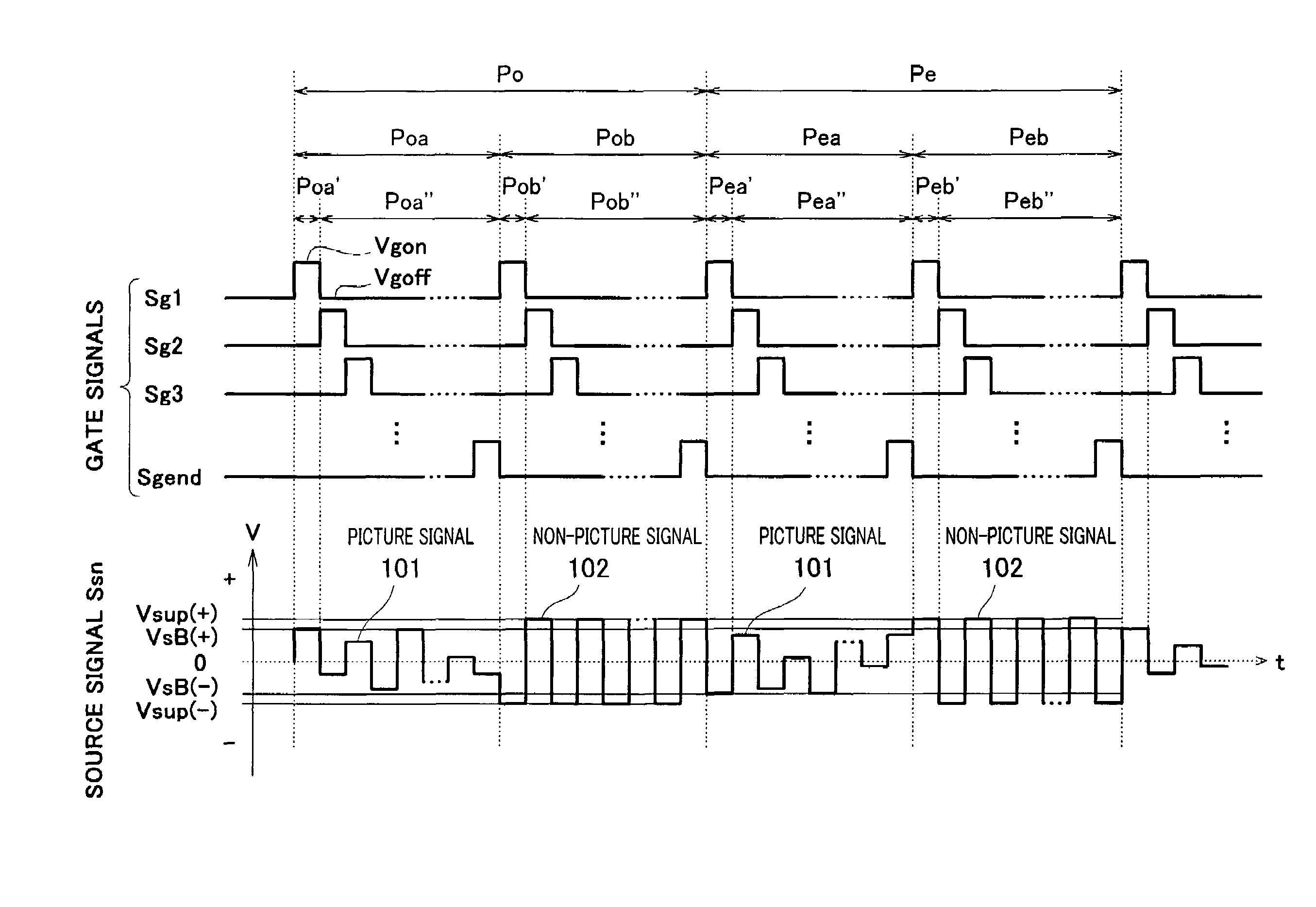
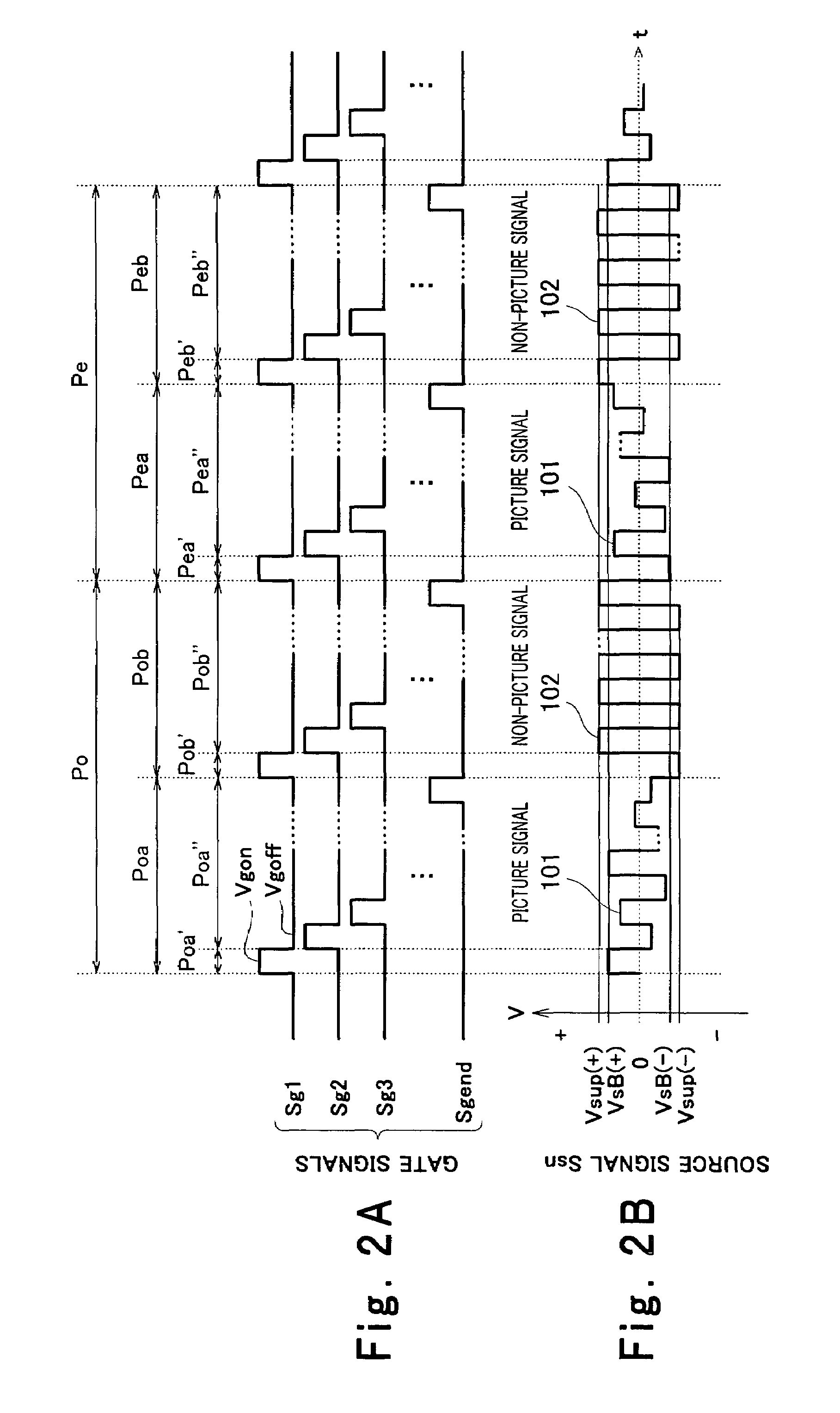
[0072]FIGS. 6A and 6B constitute a timing chart showing contents of gate signals and a source signal in a liquid crystal display device according to the second embodiment of the invention, wherein FIG. 6A is a graph showing the gate signals and FIG. 6B is a graph showing the source signal. In FIGS. 6A and 6B, the reference numerals identical to those of FIGS. 2A and 2B denote components identical or equivalent to those of FIGS. 2A and 2B.

[0073]As shown in FIGS. 6A and 6B, unlike the first embodiment, a polarity of the picture signal 101 of the source signal Ssn remains unchanged during each of frame periods Po and Pe and a polarity of a non-picture signal 102 remains unchanged during each of the frame periods Po and Pe in this embodiment. Other parts of constitution are the same as the first embodiment.

[0074]With such constitution, an amplitude of the source signal Ssn during the write periods Poa and Pea of the picture signal 101 and the write periods Pob and Peb of the non-picture...

third embodiment

[0075]FIGS. 7A and 7B constitute a timing chart showing contents of gate signals and a source signal in a liquid crystal display device according to a third embodiment of the invention, wherein FIG. 7A is a graph showing the gate signals and FIG. 7B is a graph showing the source signal. In FIGS. 7A and 7B, the reference numerals identical to those of FIGS. 2A and 2B denote components identical or equivalent to those of FIGS. 2A and 2B.

[0076]As shown in FIGS. 7A and 7B, unlike the first embodiment, each of the pixel write periods Poa′ and Pea′ of the picture signal 101 is provided twice in each of the frame periods Po and Pe in this embodiment. In this case, the picture signal 101 to be written to the pixel is actually written in each of the latter pixel write periods. Other parts of constitution are the same as the first embodiment.

[0077]With such constitution, the write period for the picture signal 101 is effectively increased, thereby further improving the ability of writing the ...


PUM


Abstract

A liquid crystal display element driving method or a liquid crystal display device uses a liquid crystal display element having a plurality of pixels constituting a screen; divides a frame period into a plurality of write periods and outputs gate signals to select the pixels sequentially during the write periods; forms each of source signals such that the source signal includes a picture signal and a non-picture signal respectively assigned for the write periods; writes each of the source signals corresponding to the selected pixels to each of the pixels with its polarity being alternated; and displays an image responsive to the source signals on the screen of the liquid crystal display element in such a manner that a transmittivity of liquid crystals of each of the pixels is controlled in accordance with the written source signal, wherein the non-picture signal having a polarity identical to that of the picture signal to be written subsequently is written to the pixels.

Description

TECHNICAL FIELD[0001]The present invention relates to a method of driving a liquid crystal display element and a liquid crystal display device using the method and, particularly, to the liquid crystal display device employing a liquid crystal mode capable of achieving a high speed response and a wide angle of visibility.BACKGROUND ART[0002]An active matrix type liquid crystal display using a thin film transistor (TFT) is used in various fields such as a display of a camcorder and a display of a personal computer or a personal word processor owing to its advantages such as a reduced thickness, a reduced weight, and capability of low voltage driving, and there is a large market for such liquid crystal display.[0003]In recent years, particularly, the liquid crystal display has been used for displaying dynamic images and has been applied to televisions in addition to the conventional use for displaying static images in a personal computer and the like, and there is an increasing demand ...

Claims


Application Information

Patent Timeline
IPC IPC(8): G09G3/36
CPCG09G3/3614G09G3/3648G09G3/3677G09G2300/0491G09G2310/0205G09G2320/0261G09G2310/0251G09G2310/06G09G2310/061G09G2320/0252G09G2320/0257G09G2310/0235G02F1/133
Inventor KIMURA, MASANORISATO, ICHIROKUMAGAWA, KATSUHIKO
Owner JAPAN DISPLAY CENT INC
Learn More