Unlock instant, AI-driven research and patent intelligence for your innovation.

Defect classification/inspection system

a technology of classification and inspection system, applied in the field of defect classification/inspection system, can solve the problems of requiring much more time and labor for accurate classification, affecting the accuracy of classification, and increasing the chance of faulty classification, so as to achieve high classification accuracy

Inactive Publication Date: 2007-01-30
SONY MFG SYST
View PDF11 Cites 23 Cited by
  • Summary
  • Abstract
  • Description
  • Claims
  • Application Information

AI Technical Summary

Benefits of technology

[0015]It is an object of the present invention to provide a defect classification / inspection system with high classification accuracy.
[0016]According to the present invention, by reducing the operator's participation in the database preparation, a database containing defect groups reduced with similarity in defect characteristics can be easily constructed, and in the classification execution process, defects are classified on a plurality of hierarchical levels.
[0018]In the defect classification / inspection system according to the present invention, defects having similar characteristics are regrouped by the defect classifying means on the basis of the characteristics information digitized by the characteristics extracting means with respect to the defects belonging to the defect group selected and designated by the selecting / designating means, and a database can be prepared in which the defects of the inspection object are hierarchically classified. Moreover, in the defect classification / inspection system according to the present invention, since the defects having similar characteristics are grouped by the defect classifying means on the basis of the characteristics information digitized by the characteristics extracting unit, the operator can easily prepare a database simply by determining whether or not the defect group only consists of single defects and providing an identification code thereto. By creating the database so it is organized in a plurality of hierarchical levels, it is possible to eliminate the similarity between the classification groups.

Problems solved by technology

In forming such a device pattern, a dust particle might stick to the surface of the semiconductor wafer or the semiconductor wafer might be scratched, thus causing a defect thereon.
The semiconductor device having such a defect generated thereon is a defective device, which lowers the yield.
However, with the design rules for semiconductor wafers growing ever smaller, various types of defects are generated, requiring much more time and labor for carrying out accurate classification.
When the difference in defect characteristics between the defect groups contained in the database is small, the chance of faulty classification increases.
Therefore, the classification requires skills and it is difficult to eliminate the similarity in defect characteristics between the classification groups contained in the database.
In the classification execution process, since all the defects are classified on a single level, the classification accuracy is lowered and classification errors easily occur.

Method used


Image

  • Defect classification/inspection system
  • Defect classification/inspection system
  • Defect classification/inspection system

Examples


Embodiment Construction

[0025]A preferred embodiment of the present invention will now be described in detail with reference to the drawings.

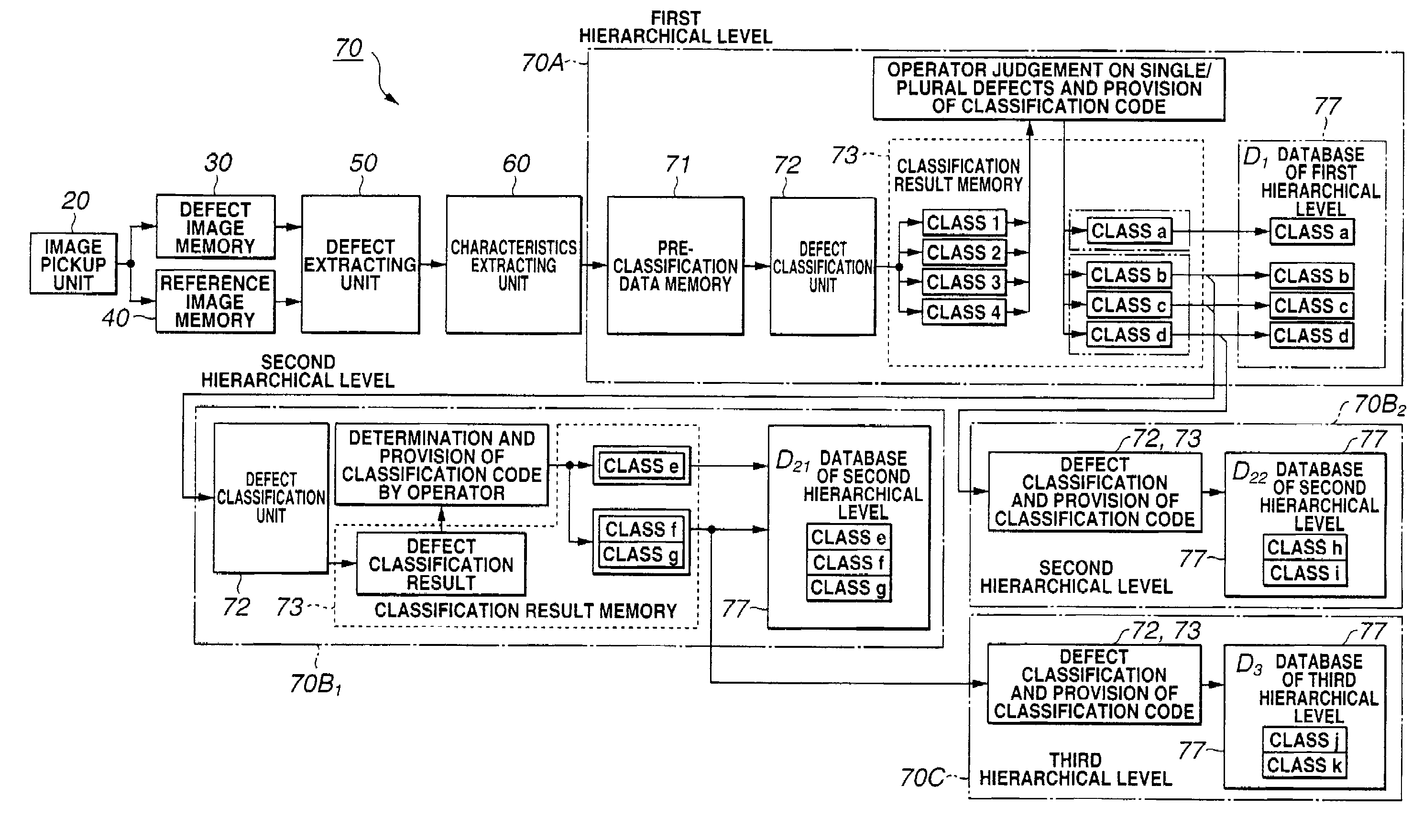
[0026]This invention is applied to, for example, a defect classification / inspection system 100 as shown in FIG. 3.

[0027]This defect classification / inspection system 100 is adapted for classifying and inspecting a defect on a semiconductor wafer 90 set on a carrier stage 10 as an inspection object. The defect classification / inspection system 100 is constituted by the carrier stage 10 controlled by a stage control unit 1, an image pickup unit 20 controlled by an image pickup control unit 2, and a defect image memory 30, a reference image memory 40, a defect extracting unit 50, a characteristics extracting unit 60, a database preparing unit 70 and a classification executing unit 80 which are controlled by a data processing control unit 3.

[0028]In this defect classification / inspection system 100, the carrier stage 10 is controlled by the stage control unit 1 and positions...


PUM


Abstract

An image of an inspection object is picked up by an image pickup unit, and a characteristics quantity of an image of a defect part extracted by a defect extracting unit is extracted and digitized by a characteristics extracting unit. A database preparing unit regroups defects having similar characteristics by a defect classification unit on the basis of the characteristics information digitized by the characteristics extracting unit with respect to defects belonging to a defect group selected and designated by an operator via a display / input unit, and prepares on a database memory a database in which the defects of the inspection object are hierarchically classified. A classification executing unit hierarchically classifies the defects of the inspection object with reference to the database provided by the database preparing unit on the basis of the digitized characteristics information extracted by the characteristics extracting unit from the image of the defect part of the inspection object extracted by the defect extracting unit. Thus, a defect classification / inspection system having high classification accuracy is provided.

Description

BACKGROUND OF THE INVENTION[0001]1. Field of the Invention[0002]This invention relates to a defect classification / inspection system for classifying and inspecting a defect of a semiconductor wafer or the like.[0003]2. Description of the Related Art[0004]A semiconductor device is prepared by forming a fine device pattern on a semiconductor wafer. In forming such a device pattern, a dust particle might stick to the surface of the semiconductor wafer or the semiconductor wafer might be scratched, thus causing a defect thereon. The semiconductor device having such a defect generated thereon is a defective device, which lowers the yield.[0005]Therefore, in order to stabilize the yield on the manufacturing line at a high standard, it is preferred to early find a defect generated by a dust particle or scratch, specify the cause of the defect, and take effective measures for the manufacturing equipment and the manufacturing process.[0006]If a defect is found, a defect inspection system is u...

Claims


Application Information

Patent Timeline
IPC IPC(8): G06K9/00G06K9/60G06K9/70G01N21/956G06F17/30G06T1/00G06T7/00
CPCG06T7/001G06T2207/30148H01L22/00
Inventor KONDO, HIROSHIOKUYAMA, MASATSUGUSAITO, YO
Owner SONY MFG SYST
Features
  • R&D
  • Intellectual Property
  • Life Sciences
  • Materials
  • Tech Scout
  • Unparalleled Data Quality
  • Higher Quality Content
  • 60% Fewer Hallucinations
Learn More