Method of manufacturing an on-chip transformer balun

a transformer and balun technology, applied in the field of radio communication technology, can solve the problems of low quality, limited integration, and small size and resistan

Inactive Publication Date: 2007-02-06
AVAGO TECH WIRELESS IP SINGAPORE PTE
View PDF10 Cites 58 Cited by
  • Summary
  • Abstract
  • Description
  • Claims
  • Application Information

AI Technical Summary

Problems solved by technology

However, such integration has been limited due to flux leakage, capacitive coupling limits, and significant series resistance.
While coplanar interleaved transformers reduces size and resistance and are widely used, they suffer from low quality (Q) factor, small coupling coefficients, and, if used as a balun, the center tap is often at an undesirable location, resulting in an asymmetric geometry.
As is known, asymmetry of a transformer winding causes an imbalance in the resulting differential signal and / or an imbalance in the resulting single ended signal from a differential signal.
While such toroidal and concentric transformers are well suited for multi-layer structures, they suffer from weak coupling, inconvenient center tap locations, and are asymmetrical.
Such transformers have high coupling coefficients and relatively small area; however, the secondary is asymmetrical creating a loading asymmetry.

Method used


Image

  • Method of manufacturing an on-chip transformer balun
  • Method of manufacturing an on-chip transformer balun
  • Method of manufacturing an on-chip transformer balun

Examples


Embodiment Construction

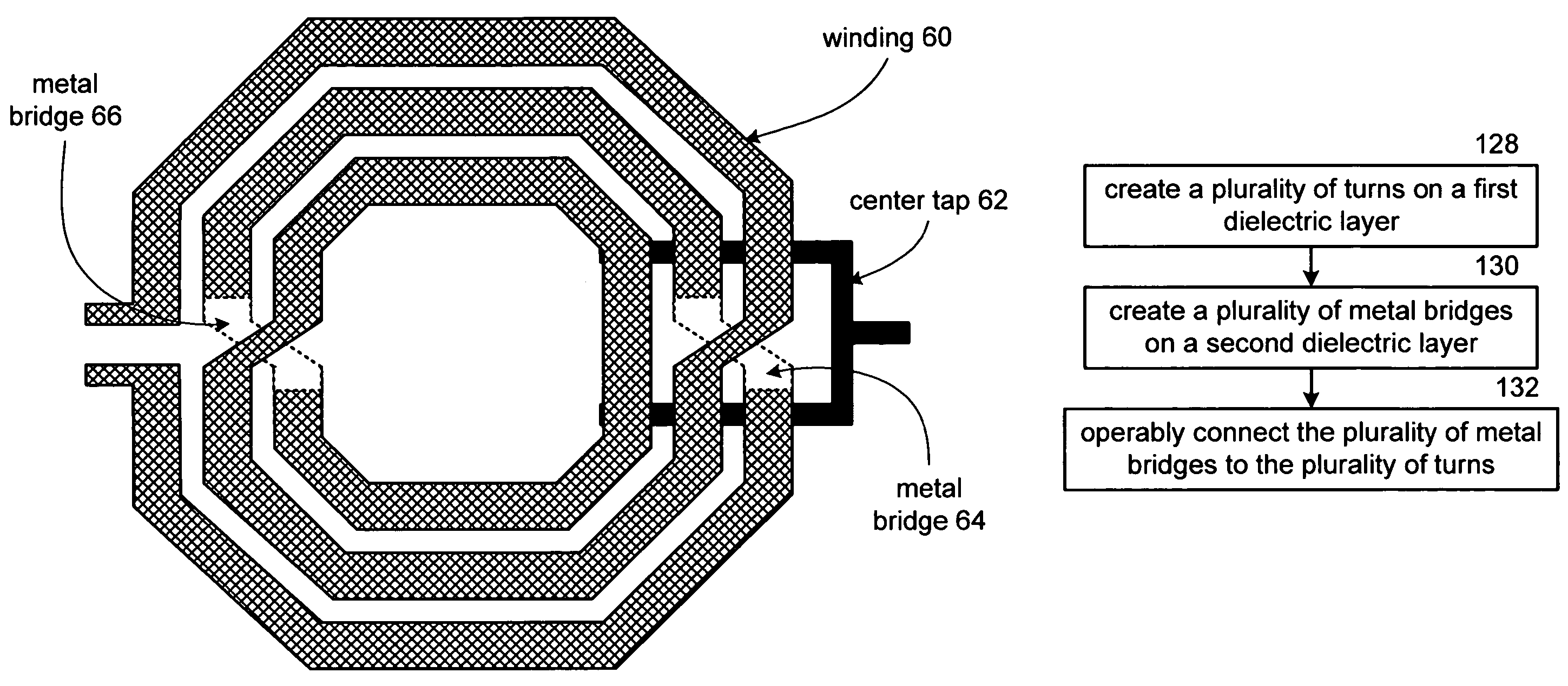
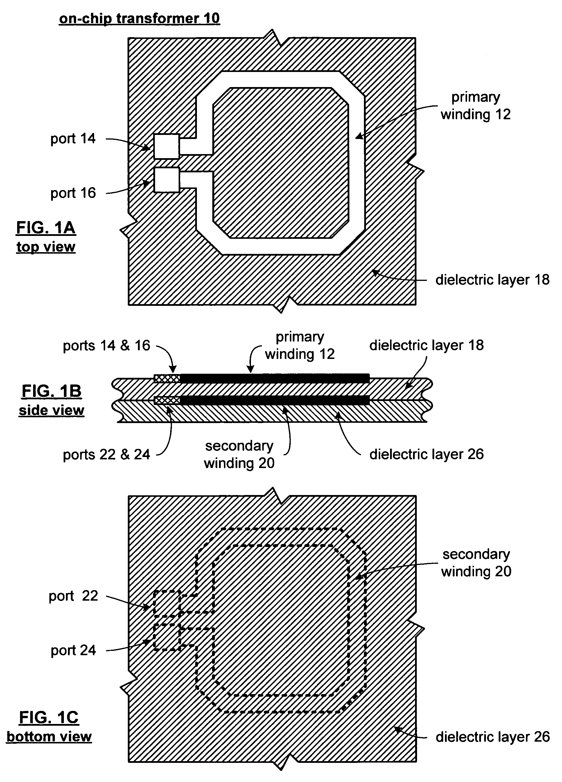
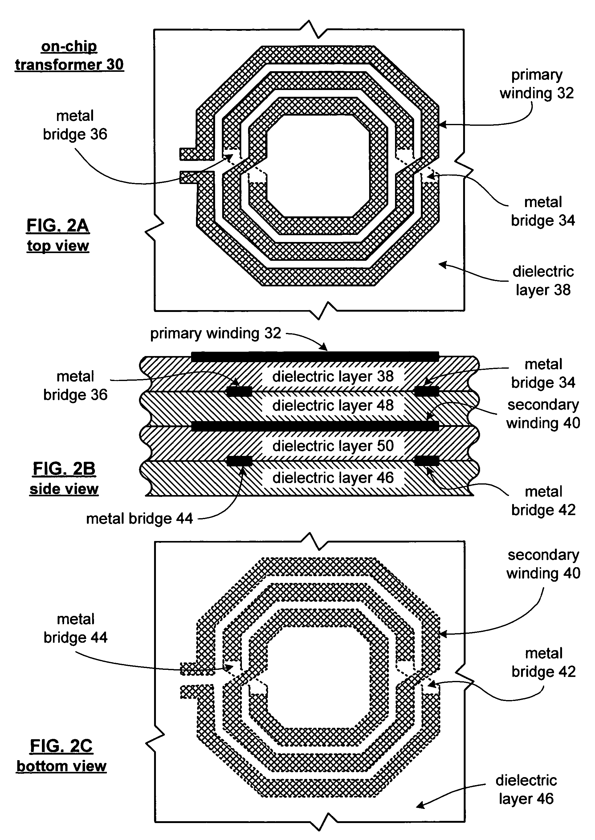
[0016]Generally, the present invention provides a transformer balun that is symmetrical in structure, provides high current, or high voltage, amplification, and has high coupling coefficients while maintaining minimal overall size. The balun structure includes primary and secondary metal windings at separate layer interfaces. The primary and secondary metal windings are symmetrical and can have any number of turns, which is only limited by integrated circuit area and capacitance. Accordingly, the primary and secondary windings may be on as many layers as needed. Further, the primary and / or secondary may include a center tap ground, which enables the winding to be used as a differential port. Such a transformer balun is well suited for radio frequency integrated circuits since it provides a symmetrical and balanced on-chip transformer.

[0017]The present invention can be more fully described with reference to FIGS. 1–9. FIGS. 1A–1C illustrate a top, side, and bottom view of an on-chip ...


PUM

PropertyMeasurementUnit
series resistanceaaaaaaaaaa
sizeaaaaaaaaaa
resistanceaaaaaaaaaa

Abstract

A method of manufacturing an on-chip transformer balun includes creating, on a semiconductor substrate, a primary winding having at least one substantially symmetrical primary turn on a first dielectric layer and at least one metal bridge on a second layer. A secondary winding is created on the semiconductor substrate, the secondary winding having at least one substantially symmetrical secondary turn on a third dielectric layer and at least one metal bridge on a fourth dielectric layer. In an alternative embodiment, the primary winding has at least one first primary turn on a first dielectric layer and at least one second primary turn on a second dielectric layer and at least one via that operably connects the first primary turn to the second primary turn. The secondary winding has at least one first secondary turn on a third dielectric layer and at least one second secondary turn on a fourth dielectric layer.

Description

[0001]This patent application is claiming priority under 35 USC § 121 to patent application entitled On-Chip Transformer balun having a Ser. No. 10 / 055,425 and a filing date of Jan. 23, 2002, which is U.S. Pat No. 6,801,114.TECHNICAL FIELD OF THE INVENTION[0002]This invention relates generally to radio communication technology and in particular to transformers used within radios.BACKGROUND OF THE INVENTION[0003]Two-way radios, which may be incorporated in wireless communication devices, are known to include an antenna, a transformer, an antenna switch, a receiver section, and a transmitter section. The antenna switch couples either the receiver section or the transmitter section to the antenna via the transformer. The transformer may be a transformer balun (balanced / unbalanced) and is generally used to convert single ended signals into differential signals and conversely to convert differential signals into single ended signals. For example, received RF signals via the antenna are c...

Claims


Application Information

Patent Timeline
Patent Type & Authority Patents(United States)
IPC IPC(8): H01F7/06H01F17/00H01F19/04H03H7/42
CPCH01F17/0013H03H7/42H01L23/5227H01L23/645H01F19/04H01F2021/125Y10T29/49135H01L2924/0002Y10T29/4902H01L2924/00
Inventor YANG, HUNG YU DAVIDCASTANEDA, JESSE A.ROFOUGARAN, REZA
Owner AVAGO TECH WIRELESS IP SINGAPORE PTE
Why Eureka
Try Eureka