Organic light emitting element and display device using the element

a technology of light emitting elements and display devices, which is applied in the direction of discharge tubes/lamp details, organic semiconductor devices, discharge tubes/lamp details, etc., can solve the problems of extremely low emission efficiency, achieve the effect of reducing the brightness of triplet light emitting elements, and prolonging the life of elements

Inactive Publication Date: 2007-02-06
SEMICON ENERGY LAB CO LTD
View PDF81 Cites 70 Cited by
  • Summary
  • Abstract
  • Description
  • Claims
  • Application Information

AI Technical Summary

Benefits of technology

[0022]The present invention has been made in view of the above, and an object of the present invention is therefore to suppress reduction in brightness of a triplet light emitting element for red color and to lengthen a life of the element, and another object of the present invention is to provide an organic light emitting element for red color with higher light emission efficiency and a longer life.
[0023]Further, still another object of the present invention is to provide a display device, in which a balance of three primary colors of light is more favorable, besides, power consumption is lower, and a change of fluctuation among colors with time is smaller than prior art, by using the triplet light emitting element for red color and singlet light emitting elements for green color and blue color. Furthermore, yet still another object of the present invention is to provide an electric device with lower power consumption than prior art and a display portion exhibiting a clear display that never fades even with the lapse of time, by using the display device.
[0024]Regardless of the difference between the singlet light emitting element and the triplet light emitting element, an organic light emitting element generally has a characteristic that a lamination structure (hetero structure) as shown in Reference 1 is formed. In Reference 1, for example, a single hetero structure, in which a hole transporting layer composed of an aromatic diamine compound and an electron transporting light emitting layer composed of tris (8-quinolinolate)-aluminum (hereinafter referred to as “Alq3”) are laminated, is applied to an organic compound film, whereby carrier recombination efficiency is enhanced steeply. This is described as follows.

Problems solved by technology

Thus, the emission efficiency is extremely low.

Method used


Image

  • Organic light emitting element and display device using the element
  • Organic light emitting element and display device using the element
  • Organic light emitting element and display device using the element

Examples


embodiments

[Embodiment 1]

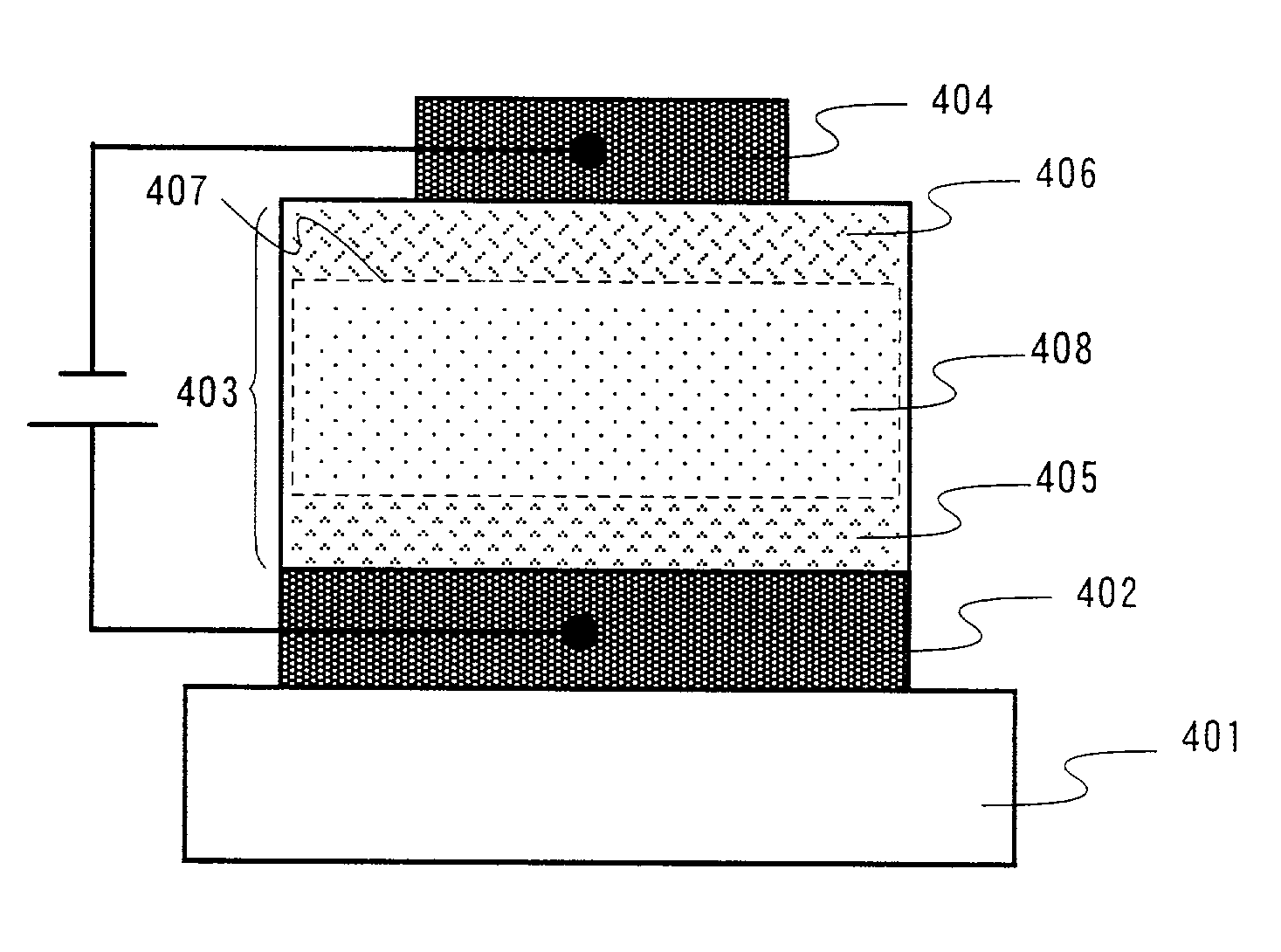
[0109]In this embodiment, an organic light emitting element shown in FIG. 4A, in which an electron injecting region composed of an electron injecting material is inserted between a cathode 404 and an organic compound film 403 is specifically exemplified.

[0110]First, ITO is deposited into a film with a thickness of approximately 100 nm by sputtering, and a glass substrate 401 on which an anode 402 is formed is prepared. The glass substrate 401 having the anode 402 is carried into the vacuum tank as shown in FIGS. 7A and 7B. In this embodiment, five evaporation sources are needed since five kinds of materials (four kinds corresponding to organic compounds and one kind corresponding to metal to be a cathode) are evaporated.

[0111]Then, α-NPD that is the hole transporting material is evaporated at an evaporation rate of 3 Å / s to form a hole transporting region with a thickness of 40 nm. Thereafter, while the evaporation rate for α-NPD is fixed at 3 Å / s, evaporation of BAlq2...

embodiment 2

[Embodiment 2]

[0114]In this embodiment, an organic light emitting element shown in FIG. 5 is specifically exemplified.

[0115]First, ITO is deposited into a film with a thickness of approximately 100 nm by sputtering, and a glass substrate 501 on which an anode 502 is formed is prepared. The glass substrate 501 having the anode 502 is carried into a vacuum tank as shown in FIGS. 7A and 7B. In this embodiment, eight evaporation sources are needed since eight kinds of materials (seven kinds corresponding to organic compounds and one kind corresponding to metal to be a cathode) are evaporated.

[0116]Then, after CuPc that is the hole injecting material is evaporated by 10 nm to form a hole injecting region 503, the evaporation of α-NPD that is the hole transporting material is started while CuPc is vaporized, whereby a mixed region 511 composed of CuPc and α-NPD is formed. The mixed region 511 is set to have a thickness of 10 nm.

[0117]Next, the evaporation of CuPc is stopped, and only α-NP...

embodiment 3

[Embodiment 3]

[0122]In this embodiment, the structure of each pixel of the display device shown in FIGS. 9A to 9E, is specifically exemplified. The evaporation device shown in FIG. 8 is used as the evaporation device to thereby form each pixel. Note that the reference numerals in FIG. 8 and FIGS. 9A to 9E are referred herein below.

[0123]First, the substrate shown in FIG. 9A is carried into the evaporation chamber 801 for red pixel, and a triplet light emitting element for red color as shown in FIG. 10A is manufactured. Here, CuPc is the hole injecting material, α-NPD is the hole transporting material. BAlq2 is the electron transporting material, and Alq3 is the electron injecting material. PtOEP is doped into a mixed region composed of α-NPD and BAlq2. The weight ratio thereof is set to α-NPD:BAlq2:PtOEP=20:80:4. Note that attention is paid to in order that intervals are not occurred between CuPc and α-NPD and between BAlq2 and Alq3 to thereby prevent the formation of an impurity la...


PUM


Abstract

A hole transporting region made of a hole transporting material, an electron transporting region made of an electron transporting material, and a mixed region (light emitting region) in which both the hole transporting material and the electron transporting material are mixed and which is doped with a triplet light emitting material for red color are provided in an organic compound film, whereby interfaces between respective layers which exist in a conventional lamination structure are eliminated, and respective functions of hole transportation, electron transportation, and light emission are exhibited. In accordance with the above-mentioned method, the organic light emitting element for red color can be obtained in which power consumption is low and a life thereof is long. Thus, the display device and the electric device are manufactured by using the organic light emitting element.

Description

BACKGROUND OF THE INVENTION[0001]1. Field of the Invention[0002]The present invention relates to an organic light emitting element which has an anode, a cathode and a film comprising an organic compound in which light emission is obtained by applying an electric field (hereinafter referred to as organic compound film), and to a display device using the organic light emitting element. The present invention particularly relates to a display device including organic light emitting elements for emitting light of respective colors of red, green and blue as pixels, in which emission efficiency of the element for emitting red color light is high and also, the element life is long. Note that the display device in this specification indicates an image display device using an organic light emitting element as a light emitting element. Further, a module in which an organic light emitting element is attached to a connector, for example, an anisotropic conductive film (FPC: flexible printed circ...

Claims


Application Information

Patent Timeline
Patent Type & Authority Patents(United States)
IPC IPC(8): H01J1/62H05B33/14H01L27/32H01L51/50
CPCH01L27/3211H01L51/5016H01L51/5048H01L51/5008H01L27/3244H01L27/3281H01L2251/5384H01L51/5096H10K59/35H10K59/12H10K59/17H10K30/865H10K50/11H10K2101/10H10K50/14H10K50/18H10K2101/90H05B33/14H10K2101/27
Inventor SEO, SATOSHIYAMAZAKI, SHUNPEI
Owner SEMICON ENERGY LAB CO LTD
Why Eureka
Try Eureka