Drain-extended MOS transistors and methods for making the same

a technology of extended mos transistors and mos transistors, which is applied in the direction of semiconductor devices, basic electric elements, electrical equipment, etc., can solve the problems of increasing the vertical spacing between the bottom of the p-well and the n-buried layer, unable to provide an adequate barrier to on-state punch-thru current from the source, and increasing the cost of process complexity. achieve the effect of improving the off-state and/or transient breakdown voltage performan

Active Publication Date: 2007-02-13
TEXAS INSTR INC
View PDF16 Cites 11 Cited by
  • Summary
  • Abstract
  • Description
  • Claims
  • Application Information

AI Technical Summary

Benefits of technology

[0010]One aspect of the invention provides a drain-extended MOS transistor, comprising an n-doped source formed in a semiconductor body, an n-doped drain laterally spaced from the source in the semiconductor body, an n-doped drift region, and a p-doped channel region in the semiconductor body. The channel region extends in the semiconductor body between the drift region and the source, and the drift region extends between the channel and the drain. The transistor further comprises a gate located above the channel region, and a p-doped buried layer located below the source, the channel region, and the drift region. In one example, the semiconductor body comprises a silicon substrate and an overlying epitaxial silicon layer, where the source, drain, channel region, and drift region are located in the epitaxial silicon layer, with at least a portion of the p-doped buried layer being located in the substrate. For high side devices, an n-buried layer can be formed in the substrate prior to forming the p-buried layer, wherein the p-buried layer is situated between the transistor and the n-buried layer to improve the off-state and / or transient breakdown voltage performance.

Problems solved by technology

However, the drain extension increases the resistance of the drain-to-source current path (Rdson), whereby DEMOS device designs often involve a tradeoff between high breakdown voltage BVdss and low Rdson.
Although the n-well may extend under the p-well, the n-well is typically only lightly doped, and therefore does not provide an adequate barrier to on-state punch-thru current from the source to the substrate.
However, the vertical spacing between the bottom of the p-well and the n-buried layer is more difficult to increase.
However, this is costly in terms of process complexity, particularly in forming the deep diffusions to connect the n-buried layer to the drain.

Method used


Image

  • Drain-extended MOS transistors and methods for making the same
  • Drain-extended MOS transistors and methods for making the same
  • Drain-extended MOS transistors and methods for making the same

Examples


Embodiment Construction

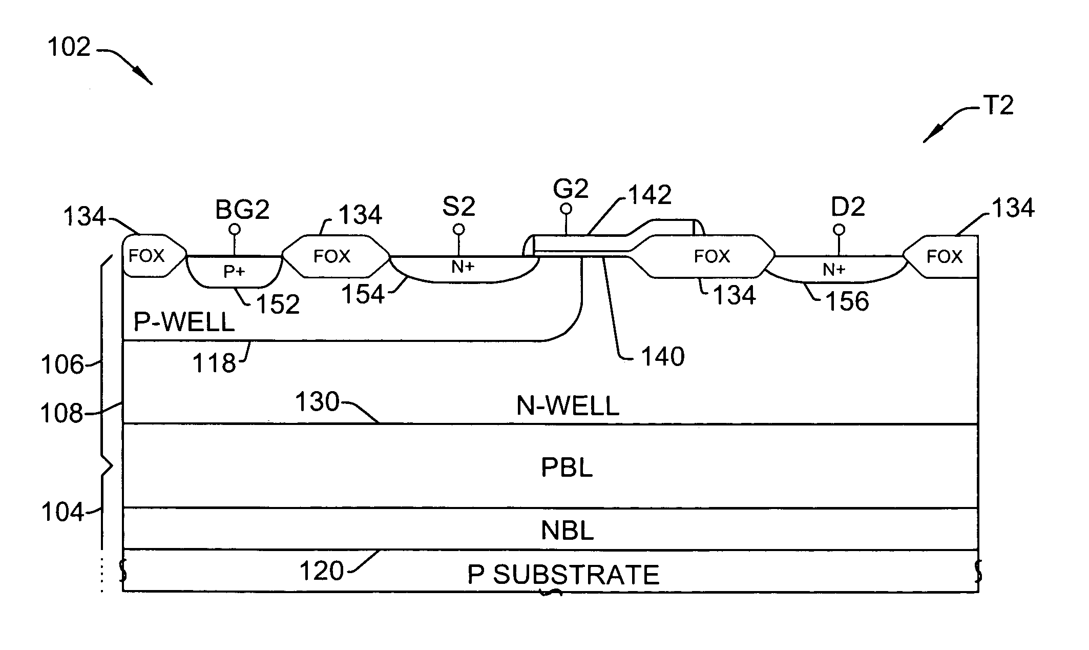
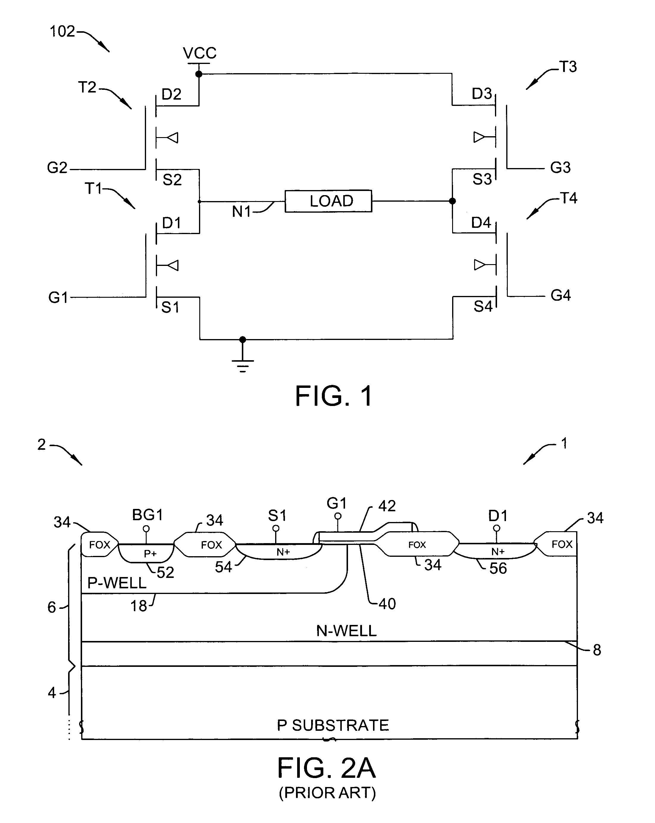
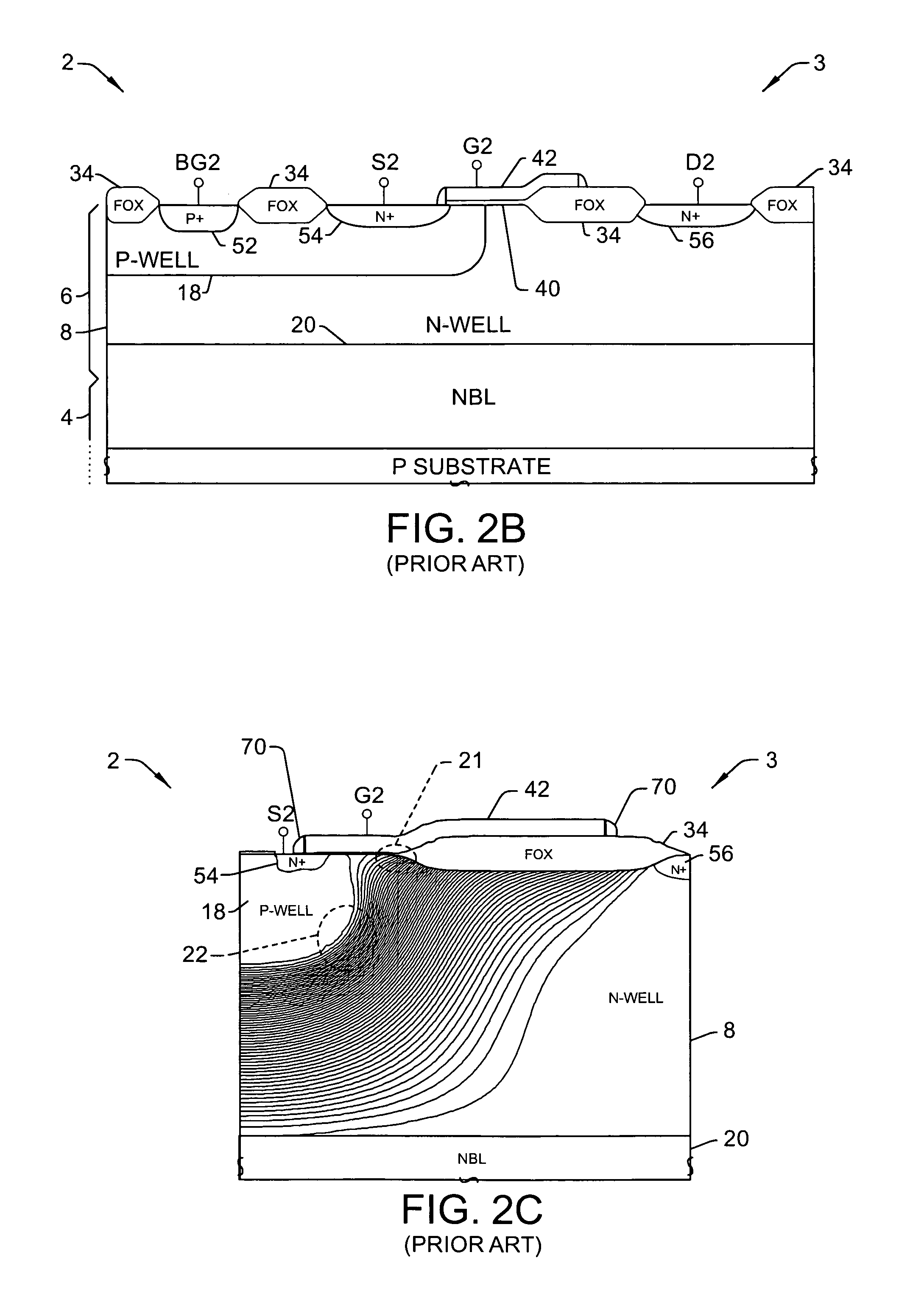
[0021]One or more implementations of the present invention will now be described with reference to the attached drawings, wherein like reference numerals are used to refer to like elements throughout, and wherein the illustrated structures are not necessarily drawn to scale. The invention provides drain-extended MOS (DEMOS) transistors and fabrication methods therefor, in which a p-buried layer is formed prior to epitaxial silicon formation over a substrate, and a drain-extended MOS transistor is formed in the epitaxial silicon layer. The p-buried layer may be formed above an n-buried layer in the substrate for high-side driver transistor applications, wherein the p-buried layer extends between the drain-extended MOS transistor and the n-buried layer to inhibit off-state or transient breakdown between the source and drain without increasing the thickness of an epitaxial silicon layer, while allowing the n-buried layer to inhibit on-state punch-thru currents between the body and the ...


PUM


Abstract

Drain-extended MOS transistors (T1, T2) and semiconductor devices (102) are described, as well as fabrication methods (202) therefor, in which a p-buried layer (130) is formed prior to formation of epitaxial silicon (106) over a substrate (104), and a drain-extended MOS transistor (T1, T2) is formed in the epitaxial silicon layer (106). The p-buried layer (130) may be formed above an n-buried layer (120) in the substrate (104) for high-side driver transistor (T2) applications, wherein the p-buried layer (130) extends between the drain-extended MOS transistor (T2) and the n-buried layer (120) to inhibit off-state breakdown between the source (154) and drain (156).

Description

[0001]This is a division of application Ser. No. 10 / 880,907, filed Jun. 30, 2004.FIELD OF INVENTION[0002]The present invention relates generally to semiconductor devices and more particularly to extended-drain MOS transistor devices and fabrication methods for making the same.BACKGROUND OF THE INVENTION[0003]Power semiconductor products are often fabricated using N or P channel drain-extended metal-oxide-semiconductor (DEMOS) transistor devices, such as lateral diffused MOS (LDMOS) devices or RESURF transistors, for high power switching applications. DEMOS devices advantageously combine short-channel operation with high current handling capabilities, relatively low drain-to-source on-state resistance (Rdson), and the ability to withstand high blocking voltages without suffering voltage breakdown failure. Breakdown voltage is typically measured as drain-to-source breakdown voltage with the gate and source shorted together (BVdss), where DEMOS device designs often involve a tradeoff b...

Claims


Application Information

Patent Timeline
Patent Type & Authority Patents(United States)
IPC IPC(8): H01L21/336
CPCH01L29/1083H01L29/7816H01L29/66689H01L29/42368
Inventor PENDHARKAR, SAMEER
Owner TEXAS INSTR INC
Why Eureka
Try Eureka