
Light emitting device

a technology of light emitting device and light emitting layer, which is applied in the direction of discharge tube luminescnet screen, discharge tube/lamp details, electric discharge lamps, etc., can solve the problems of large changes in the white balance of white light, inability to strictly control the light emitting layer of blue light emitting element b>802/b>, and inability to use the light emitting layer of indium gallium nitride as the light emitting layer of blue light emi

Inactive Publication Date: 2007-02-13
KK TOSHIBA +1
View PDF45 Cites 53 Cited by
  • Summary
  • Abstract
  • Description
  • Claims
  • Application Information

AI Technical Summary

Problems solved by technology

Therefore, the device configuration was inevitably complicated and needed troublesome adjustment.
(1) The white balance largely fluctuates among light emitting devices.
(2) The white balance largely changes with the current value supplied.
(3) The white balance largely changes with the ambient temperature.
(4) The white balance largely changes with life of the semiconductor light emitting element 802.
That is, indium gallium nitride used as the light emitting layer of the blue light emitting element 802 is difficult to control strictly, and subject to fluctuation of emission wavelength among wafers on which it grows.
It results in large changes of the white balance of the white light as the output of the device, and invites those problems, namely, fluctuation in brightness (luminance) and color (tone) of the white light obtained, bad reproducibility among products, and low mass productivity.
Moreover, the light emitting device shown in FIG. 16 inherently involves another problem that it is difficult to adjust the quantity of the fluorescent element in the resin enclosing the semiconductor element in accordance with the luminance of the light emitting element.
Especially, emission from YAG:Ce with a high visible sensitivity is difficult to control because an error in quantity of the fluorescent element in the order of several micro grams (μg) influences the tone and the luminance.
Furthermore, this light emitting device is operative only in a narrow, limitative temperature range.
That is, since the part lit “white” in the ON state looks “yellow” in the OFF state, its “appearance” is not good.

Method used


Image

  • Light emitting device
  • Light emitting device
  • Light emitting device

Examples


first embodiment

[0045](First Embodiment)

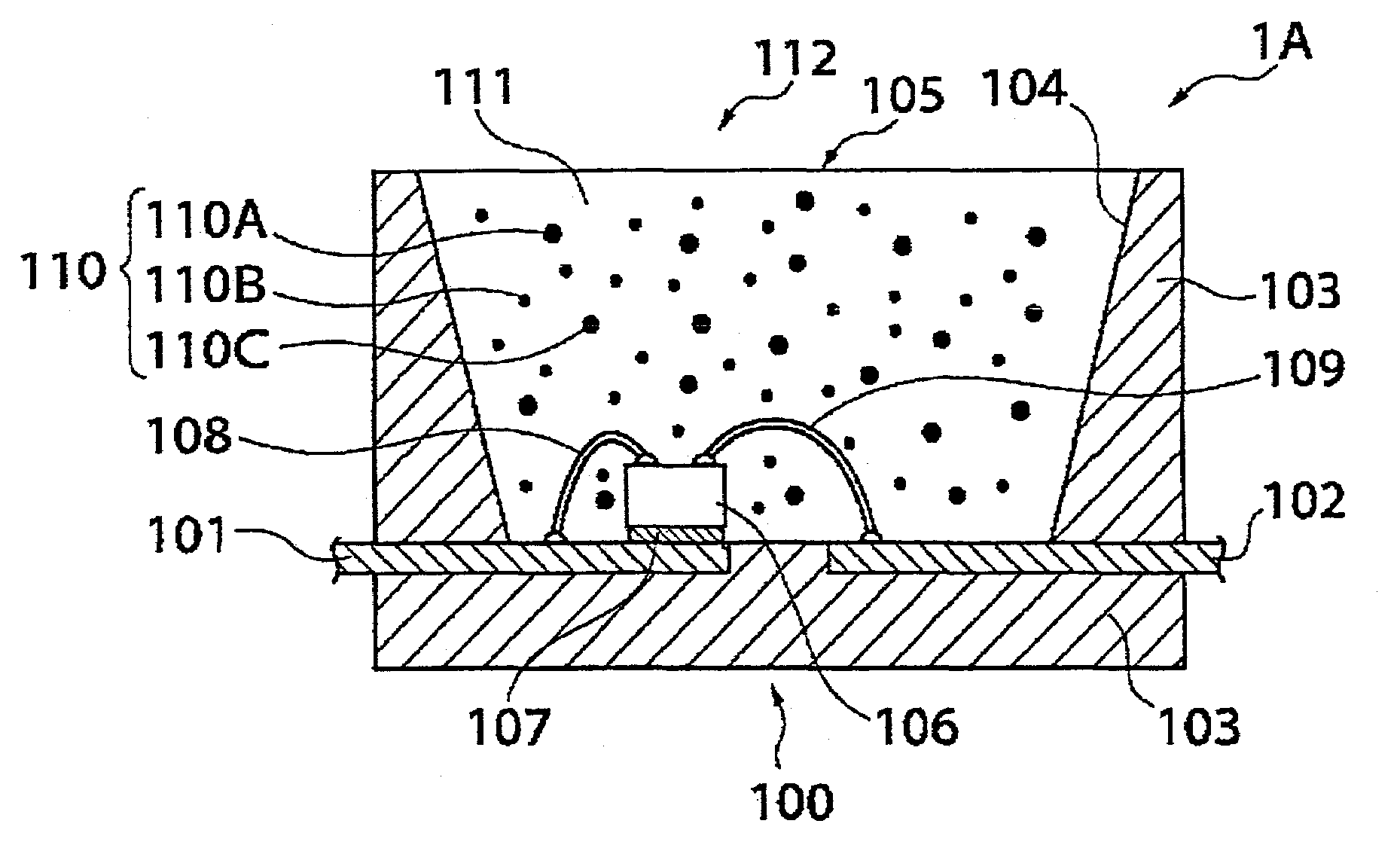
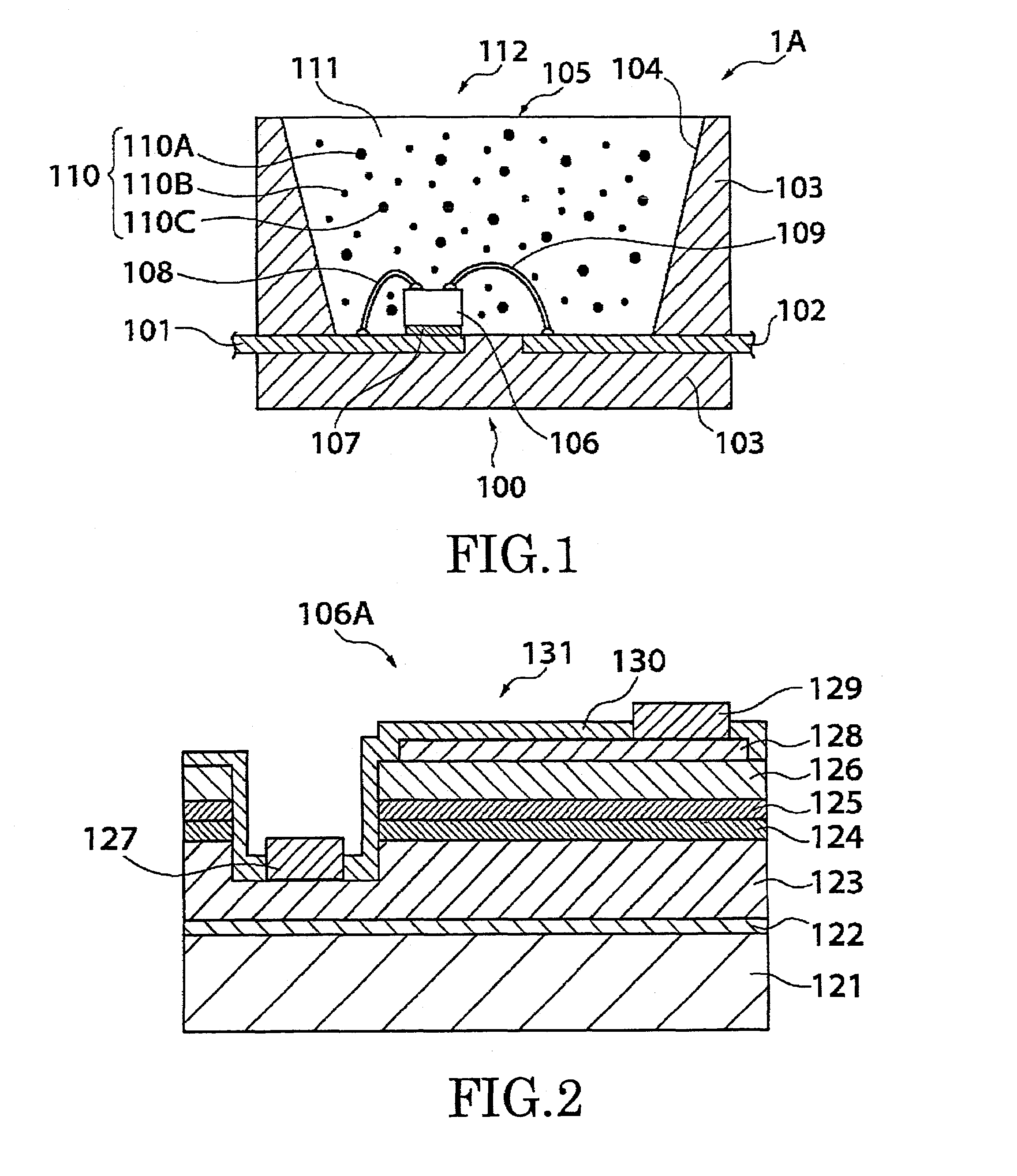
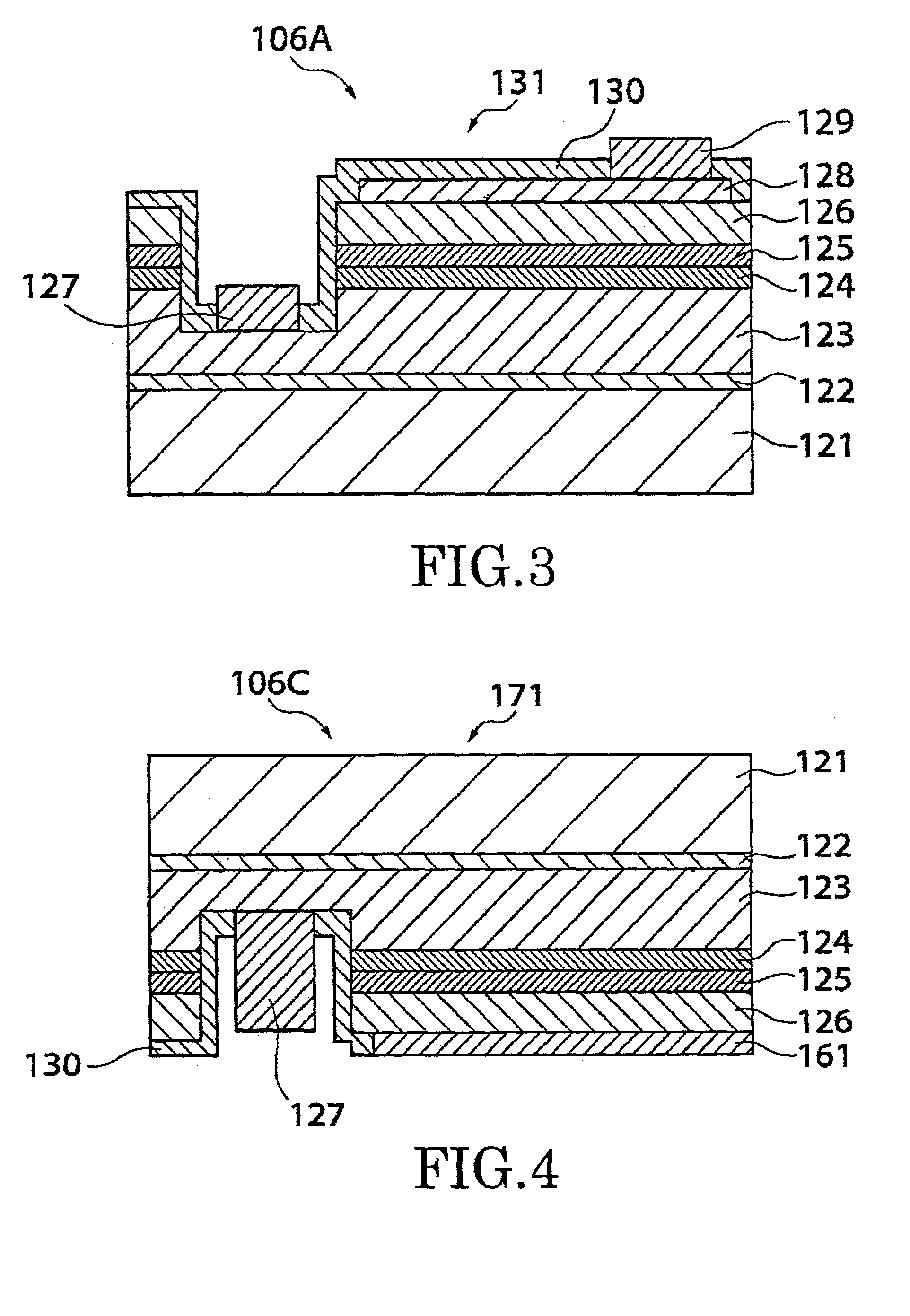
[0046]FIG. 1 is a cross-sectional view that schematically shows a configuration of the substantial part of a light emitting device according to the first embodiment of the invention.

[0047]The light emitting device 1A shown here includes a resin stem 100, a semiconductor light emitting element 106 mounted on the resin stem 100, and a sealing element 111 provided to embed the element 106.

[0048]The resin stem 100 includes leads 101, 102 shaped from a lead frame, and a resin portion 103 molded integrally with the leads 101, 102. The leads 101, 102 have opposed ends close to each other, and extend therefrom in the opposite directions to outside the resin portion 103.

[0049]The resin portion 103 has an opening 105, and the semiconductor light emitting element 106 is mounted on the bottom of the opening 105. The planar geometry of the opening 105 may be elliptical or circular, for example. The inner wall surface of the resin portion 103 surrounding the element 106 in...

second embodiment

[0218](Second Embodiment)

[0219]Next explained is the second embodiment of the invention.

[0220]FIG. 8 is a cross-sectional view that schematically shows a configuration of the substantial part of a light emitting device according to the second embodiment of the invention. Among components shown here, the same or equivalent components as those already explained with reference to FIGS. 1 through 7 are commonly labeled, and their detailed explanation is omitted for simplicity.

[0221]The light emitting device 1B shown here also includes a resin stem 100, semiconductor light emitting element 106 mounted thereon, and sealing element 111 embedding the element 106.

[0222]In this embodiment, however, the sealing element 111 containing the fluorescent element 110 merely embeds the light emitting element 106, and a second sealing element 213 of a transparent resin is provided outside the sealing element 111.

[0223]The limitative use of the sealing element 111 containing the fluorescent element onl...

third embodiment

[0227](Third Embodiment)

[0228]Next explained is the third embodiment of the invention.

[0229]FIG. 9 is a cross-sectional view that schematically shows a configuration of the substantial part of a light emitting device according to the third embodiment of the invention. Here again, the same or equivalent components as those already explained with reference to FIGS. 1 through 8 are commonly labeled, and their detailed explanation is omitted for simplicity.

[0230]The light emitting device 1C shown here also includes a resin stem 100, semiconductor light emitting element 106 mounted thereon, and sealing element 111 embedding the element 106.

[0231]Similarly to the second embodiment, the sealing element 111 containing the fluorescent element 110 merely embeds the light emitting element 106. In this embodiment, however, the space outside the sealing element 111 remains open, without being filled by any other sealing element.

[0232]Here again, the limitative use of the sealing element 111 cont...


PUM


Abstract

A light emitting device, free from change of color even when the wavelength of a light emitting element shifts, includes a light emitting element (106) for emitting primary light having an intensity peak at a wavelength shorter than 400 nm; a silicone resin (111) provided to embed the light emitting element; and a fluorescent element (110) contained in the silicone resin to absorb the primary light and release visible light.

Description

CROSS-REFERENCE TO RELATED APPLICATIONS[0001]This application is based upon and claims the benefit of priority from the prior Japanese Patent Application No. 2001-110673, filed on Apr. 9, 2001; the entire contents of which are incorporated herein by reference.BACKGROUND OF THE INVENTION[0002]This invention relates to a light emitting device, in particular, combining a light emitting element like a semiconductor light emitting element and a wavelength converting means like a fluorescent element.[0003]Light emitting devices combining LEDs (light emitting diodes) or other semiconductor light emitting elements and fluorescent elements have been remarked as inexpensive, long-lived light emitting devices, and their development is being progressed. Light emitting devices of this type have the advantage of providing emission colors conventional semiconductor light emitting elements could not realize.[0004]Usually, semiconductor light emitting elements emit light upon re-combination of carri...

Claims


Application Information

Patent Timeline
IPC IPC(8): H01L33/00H05B33/00H01L33/32H01L33/42H01L33/50H01L33/54H01L33/56H01L33/60H01L33/62
CPCH01L33/56H01L33/501H01L33/54H01L2224/32257H01L2224/32245H01L2224/45144H01L2224/48247H01L2224/48257H01L2224/73265H01L2224/48091H01L2924/00014H01L2924/00H01L2924/12032H01L2924/00012
Inventor NITTA, KOICHIOSHIO, HIROAKISHIMOMURA, KENJIKITAJIMA, TOMOKAZUTAKAHASHI, NOZOMUTAKAHASHI, YUJIUEMURA, TOSHIYAOTA, KOICHI
Owner KK TOSHIBA
Features
  • Generate Ideas
  • Intellectual Property
  • Life Sciences
  • Materials
  • Tech Scout
  • Unparalleled Data Quality
  • Higher Quality Content
  • 60% Fewer Hallucinations
Learn More