Multilayer coil component and its manufacturing method

a multi-layer coil and manufacturing method technology, applied in the direction of coil manufacturing, transformer/inductance details, inductance, etc., can solve the problems of reducing the insulating resistance between the via-holes, high disadvantages of coil conductor design b>33, etc., to achieve high relative inductance, reduce size, and thin shape

Active Publication Date: 2007-02-13
MURATA MFG CO LTD
View PDF6 Cites 15 Cited by
  • Summary
  • Abstract
  • Description
  • Claims
  • Application Information

AI Technical Summary

Benefits of technology

[0013]To overcome the problems described above, preferred embodiments of the present invention achieve a high relative inductance (L) by equalizing the inner area and the outer area of a coil conductor, while a reduced size and a thin shape are maintained. Furthermore, preferred embodiments of the present invention provide a laminated coil component which effectively prevents a decrease in insulating resistance between via-holes and also provide a method for manufacturing the same.

Problems solved by technology

As a result, it is highly disadvantageous to design a coil conductor 33 having substantially equal inner and outer areas.
Furthermore, the conductive Ag material for the via-holes 35 is easily diffused, which results in a decrease in insulating resistance between the via-holes 35.

Method used


Image

  • Multilayer coil component and its manufacturing method
  • Multilayer coil component and its manufacturing method
  • Multilayer coil component and its manufacturing method

Examples


first preferred embodiment

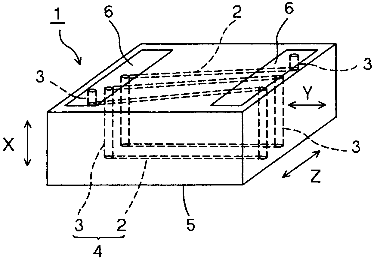
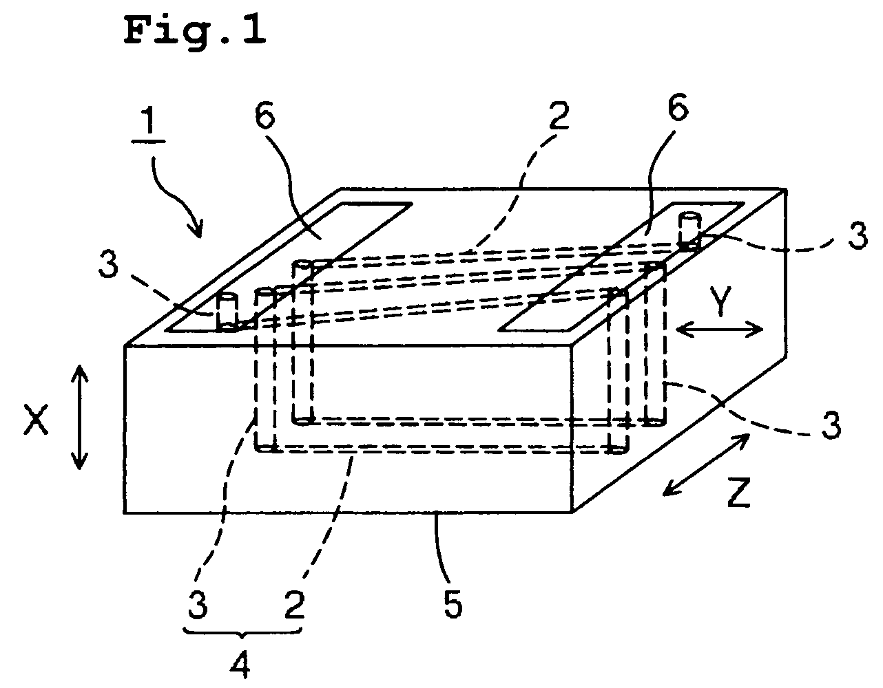
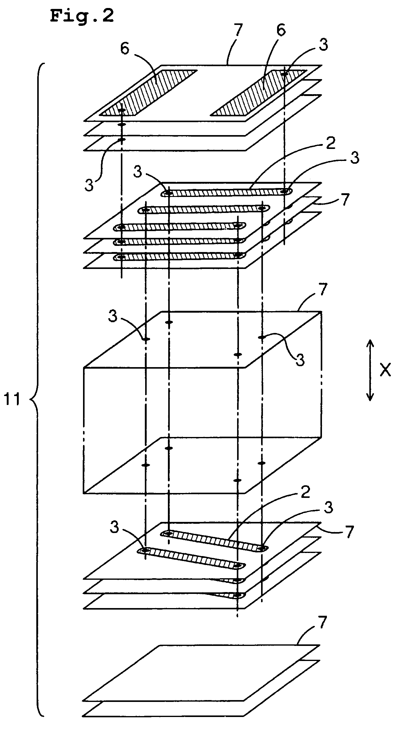
[0041]FIG. 1 is a perspective view of a chip inductor of a laminated coil component according to a first preferred embodiment. FIG. 2 is an exploded perspective view of the chip inductor. FIG. 3 is a graph showing characteristics of relative inductance (L) with an applied current. FIG. 4 is a graph showing a rate of change in relative inductance (L) with an applied current. FIG. 5 shows a relationship between a ratio of the areas and bias characteristics in a coil conductor. FIGS. 6 to 8 are side views of mounted chip inductors; FIG. 6 shows a first mounting structure, FIG. 7 shows a second mounting structure, and FIG. 8 shows a third mounting structure.

[0042]Referring to FIGS. 1 and 2, the chip inductor 1 preferably includes a coil conductor 4 including a plurality of strip electrodes 2 and a large number of via-holes 3 inside an approximately rectangular ceramic laminate 5. The via-holes 3 electrically and mechanically connect predetermined ends of the strip electrodes 2. In the c...

second preferred embodiment

[0065]FIG. 9 is a perspective view of an appearance of a chip inductor according to a second preferred embodiment of the present invention. FIG. 10 is an exploded perspective view of the chip inductor. The chip inductor is represented by reference numeral 21. The structure of the chip inductor 21 according to this preferred embodiment is preferably substantially the same as that of the chip inductor 1 according to the first preferred embodiment except for the structure of the external electrodes.

[0066]Therefore, in FIGS. 9 and 10, the same elements as those described with reference to FIGS. 1 and 2 are referred to with the same reference numerals as in FIGS. 1 and 2, and the detailed description of these elements is omitted. Since the manufacturing process and the function of the chip inductor 21 according to the second preferred embodiment are substantially the same as those of the chip inductor 1 according to the first preferred embodiment, the detailed description thereof is omit...


PUM

PropertyMeasurementUnit
thicknessaaaaaaaaaa
thicknessaaaaaaaaaa
widthaaaaaaaaaa

Abstract

A laminated coil component includes a coil conductor including a plurality of strip electrodes and via-holes inside an approximately rectangular ceramic laminate. The via-holes connect the ends of the strip electrodes. The axis of the coil conductor corresponds with the width direction Z of the ceramic laminate that is substantially perpendicular to both the laminated direction (thickness direction) X and the longitudinal direction Y of the ceramic laminate. The manufacturing process includes the steps of laminating ceramic green sheets having the strip electrodes and / or the via-holes and the ceramic green sheets having printed conductive patterns constituting external electrodes, and press-bonding and firing them.

Description

BACKGROUND OF THE INVENTION[0001]1. Field of the Invention[0002]The present invention relates to laminated coil components and methods of manufacturing the same. In particular, the present invention relates to a unique arrangement of coil conductors inside ceramic laminates.[0003]2. Description of the Related Art[0004]A longitudinally laminated and laterally coiled chip inductor disclosed in Japanese Unexamined Patent Application Publication No. 2002-252117 is an example of a laminated coil component. As shown in FIG. 11, a chip inductor 31 includes a coil conductor 33 having an axis that is perpendicular to the laminated direction (thickness direction) X inside an approximately rectangular ceramic laminate 32. The coil conductor 33 having the axis extending in the longitudinal direction Y of the ceramic laminate 32 is provided inside the ceramic laminate 32. Strip electrodes 34 are disposed at the upper portion and the lower portion inside the ceramic laminate 32. The ends of the s...

Claims


Application Information

Patent Timeline
Patent Type & Authority Patents(United States)
IPC IPC(8): H01F5/00H01F17/00H01F27/29H01F41/04
CPCH01F17/0013H01F17/0033H01F41/046H01F27/292H01F27/2804
Inventor MAEDA, EIICHITANAKA, HIROSHIYAMAMOTO, TAKAHIRO
Owner MURATA MFG CO LTD
Why Eureka
Try Eureka