
Operating non-volatile memory without read disturb limitations

a non-volatile memory and non-volatile technology, applied in the field of memory devices, can solve the problems of affecting performance, extra hardware, corrupting system code,

Active Publication Date: 2007-02-13
SANDISK TECH LLC
View PDF25 Cites 197 Cited by
  • Summary
  • Abstract
  • Description
  • Claims
  • Application Information

AI Technical Summary

Benefits of technology

This approach effectively mitigates Read Disturb by ensuring that only one word line is used for read operations, protecting the data from corruption and maintaining the integrity of stored information in memory devices.

Problems solved by technology

If the device is used long enough, the memory storing the operating system code may be subject to errors due to Read Disturb, causing the operating system code to be corrupted.
These solutions, however, may require extra hardware or may negatively impact performance.

Method used


Image

  • Operating non-volatile memory without read disturb limitations
  • Operating non-volatile memory without read disturb limitations
  • Operating non-volatile memory without read disturb limitations

Examples


Embodiment Construction

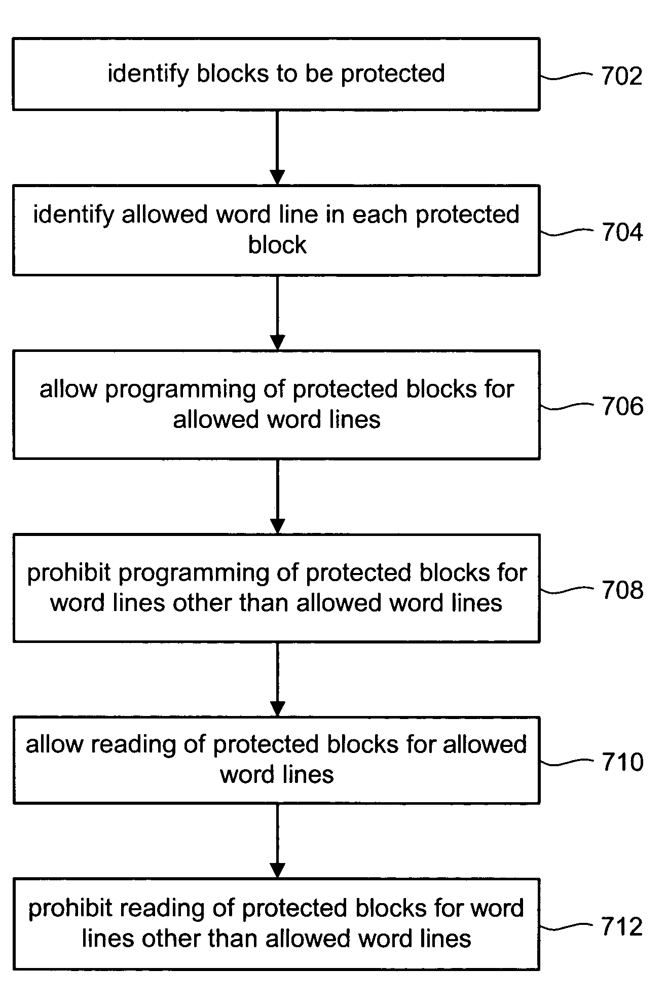
[0041]To avoid the limitations of Read Disturb, one embodiment of the present invention proposes that, for a block (or other grouping) or non-volatile storage elements, data is stored on those non-volatile storage elements associated with one word line of the block (or other grouping). The system is prohibited from storing data on those non-volatile storage elements associated with the other word lines of that block.

[0042]FIG. 5 is a block diagram of one embodiment of a flash memory system that can be used to implement the present invention. Memory cell array 302 is controlled by column control circuit 304, row control circuit 306, c-source control circuit 310 and p-well control circuit 308. Column control circuit 304 is connected to the bit lines of memory cell array 302 for reading data stored in the memory cells, for determining a state of the memory cells during a program operation, and for controlling potential levels of the bit lines to promote the programming or to inhibit th...


PUM


Abstract

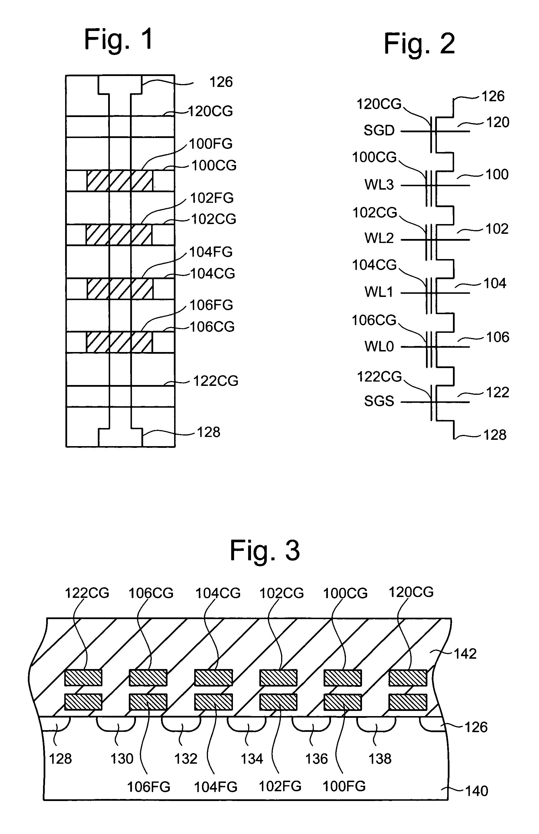
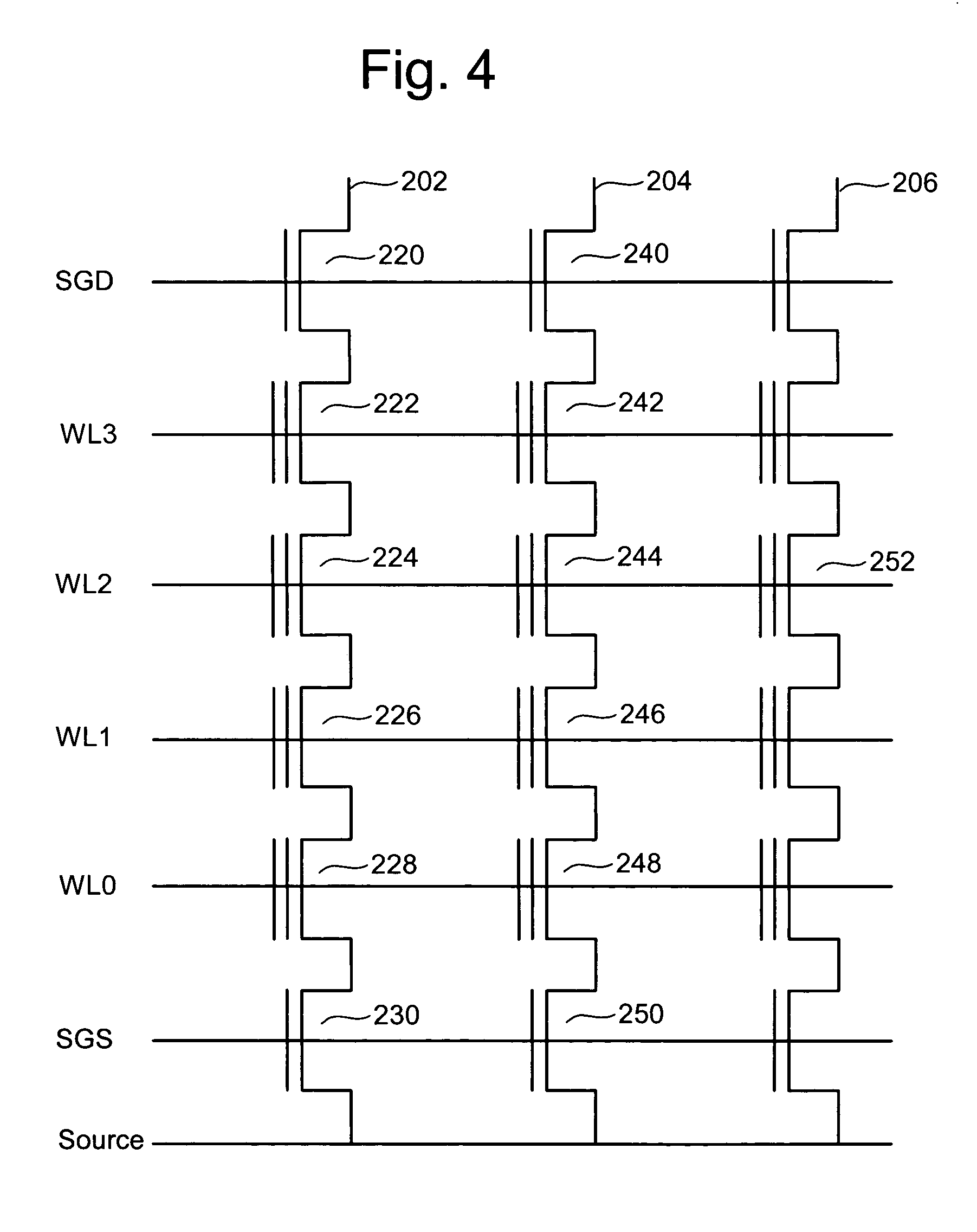
When reading a memory cell on a NAND string, the word lines for the memory cells not being read will receive a voltage so that those memory cells operate as pass gates. Over time, if there are a lot of read operations without any program operations, the cells not being read may suffer from Read Disturb because the voltage applied to the word lines may cause electrons to accumulate in the floating gates of the non-selected cells. The accumulation of charge in the floating gates raises the threshold voltage. To avoid the limitations of Read Disturb, only one word line of a block (or other grouping) is used to program and read data. In a system using NAND flash memory, the word line being read is not typically subjected to read disturb. Thus, a NAND flash memory that restricts programming and reading to one word line of a block is not likely to exhibit read disturb in that block.

Description

BACKGROUND OF THE INVENTION[0001]1. Field of the Invention[0002]The present invention relates generally to technology for memory devices and, more specifically, to operating memory devices without the limitations of read disturb.[0003]2. Description of the Related Art[0004]Semiconductor memory devices have become more popular for use in various electronic devices. For example, non-volatile semiconductor memory is used in cellular telephones, digital cameras, personal digital assistants, mobile computing devices, non-mobile computing devices, desktop computers and other devices. Electrical Erasable Programmable Read Only Memory (EEPROM) and flash memory are among the most popular non-volatile semiconductor memories.[0005]Typical EEPROMs and flash memories utilize a memory cell with a floating gate that is provided above and insulated from a channel region in a semiconductor substrate. The floating gate is positioned above and between source and drain regions. A control gate is provid...

Claims


Application Information

Patent Timeline
Patent Type & Authority Patents(United States)
IPC IPC(8): G06F12/00G11C11/56G11C16/34
CPCG11C11/5628G11C11/5642G11C16/349G11C16/3418G11C16/3427G11C16/0483
Inventor CHEN, JIANGAVENS, LEE MERRILL
Owner SANDISK TECH LLC
Learn More