PMOS device with drain junction breakdown point located for reduced drain breakdown voltage walk-in and method for designing and manufacturing such device

a technology of pmos device and breakdown point, which is applied in the direction of semiconductor device, semiconductor/solid-state device details, electrical apparatus, etc., can solve the problems of bvdss walk-in and failure of the functional pmos devi

Active Publication Date: 2007-02-20
NAT SEMICON CORP
View PDF3 Cites 45 Cited by
  • Summary
  • Abstract
  • Description
  • Claims
  • Application Information

AI Technical Summary

Problems solved by technology

Drain breakdown voltage walk-in (Bvdss walk-in) can cause functional PMOS device failure, such as during high temperature (e.g., 150° C.) o

Method used


Image

  • PMOS device with drain junction breakdown point located for reduced drain breakdown voltage walk-in and method for designing and manufacturing such device
  • PMOS device with drain junction breakdown point located for reduced drain breakdown voltage walk-in and method for designing and manufacturing such device
  • PMOS device with drain junction breakdown point located for reduced drain breakdown voltage walk-in and method for designing and manufacturing such device

Examples


Embodiment Construction

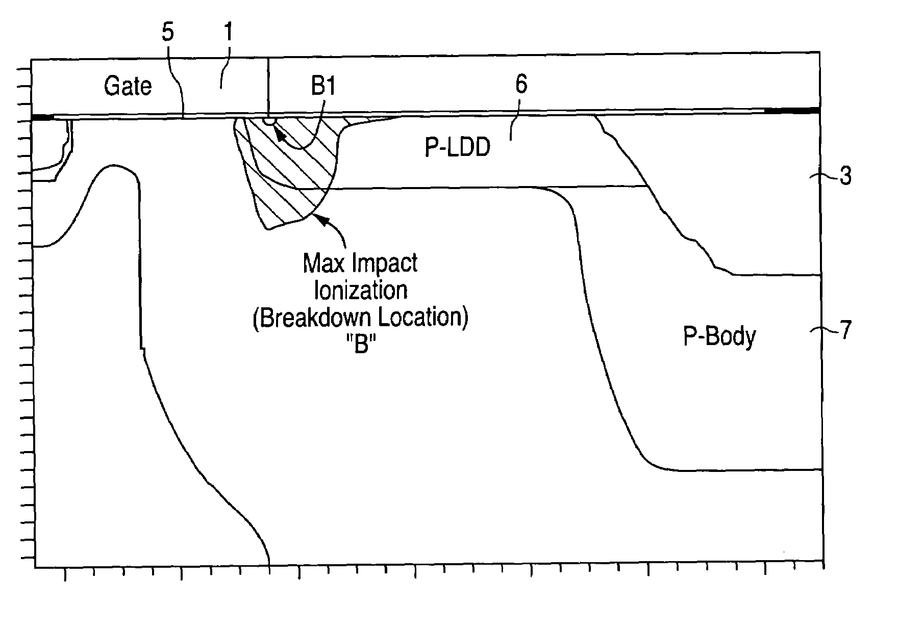
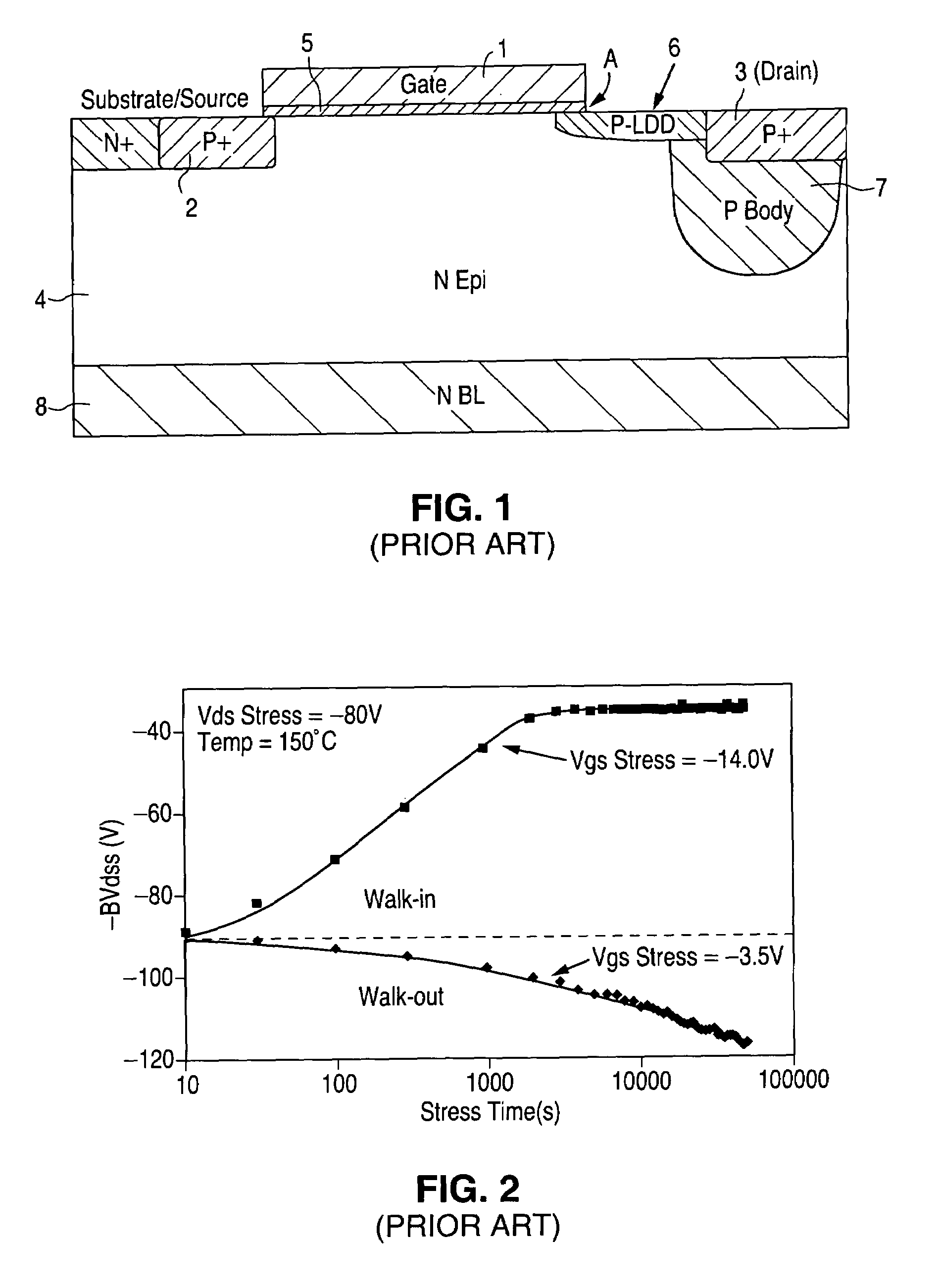
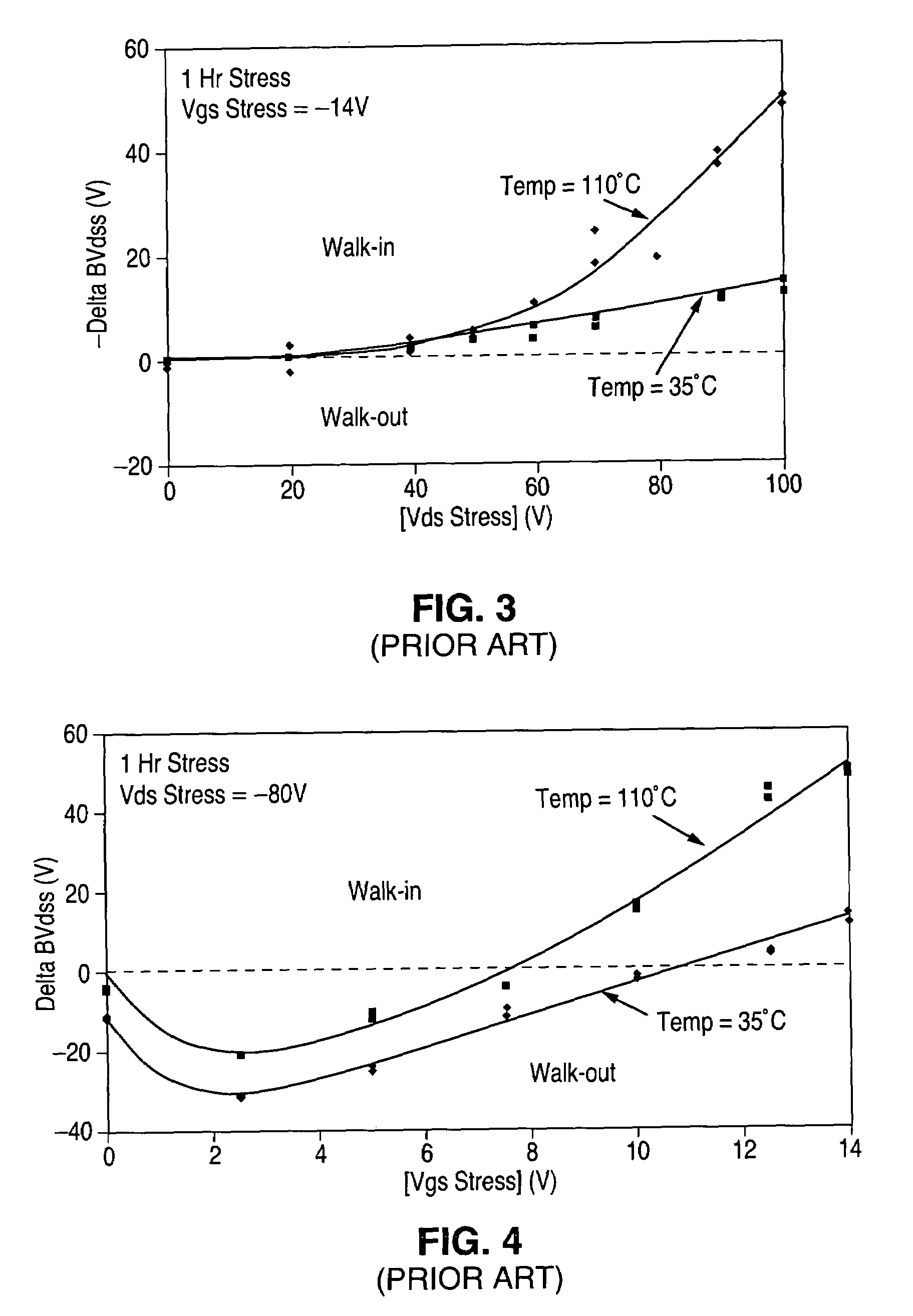
[0015]In a class of embodiments, a PMOS device is designed and manufactured in accordance with the invention such that its drain junction breakdown point and maximum impact ionization point are located to reduce Bvdss walk-in below a predetermined value. In some embodiments, a PMOS device is designed and manufactured such that both its drain junction breakdown point and maximum impact ionization point are located to be sufficiently far from its gate that the device exhibits no significant Bvdss walk-in.

[0016]In a class of embodiments, the inventive device is a high voltage PMOS power transistor (an “HV-PMOS” device) having an extended drain region. The extended drain region includes a P-type lightly doped drain (P-LDD) implant. In some such embodiments, the drain junction breakdown point and maximum impact ionization point of the device are located as desired (relative to the edge of the gate) by controlling the implant dose employed to produce the P-LDD implant. For example, in som...


PUM


Abstract

A PMOS device can be designed and manufactured in accordance with the invention to locate its drain junction breakdown point and maximum impact ionization point to reduce or eliminate drain breakdown voltage walk-in. In some embodiments, the drain junction breakdown point and maximum impact ionization point are located sufficiently far from the gate that the device exhibits no significant drain breakdown voltage walk-in. The device can be a high voltage power transistor having an extended drain region including a P-type lightly doped drain (P-LDD) implant, with drain junction breakdown and maximum impact ionization points appropriately located by controlling the implant dose employed to produce the P-LDD implant. Other aspects of the invention are methods for designing a PMOS device including by determining relative locations of the gate and at least one of the drain junction breakdown and maximum impact ionization points to reduce drain breakdown voltage walk-in, and methods for manufacturing integrated circuits including any embodiment of the PMOS device of the invention.

Description

BACKGROUND OF THE INVENTION[0001]1. Field of the Invention[0002]The present invention pertains to metal-oxide-semiconductor field effect (MOS) devices and methods for manufacturing MOS devices and integrated circuits including them. In preferred embodiments, the invention pertains to methods for manufacturing p-channel MOS devices (PMOS devices) to reduce or eliminate the dependence of their drain breakdown voltage on stress factors (e.g., temperature stress and / or voltage stress).[0003]2. Description of the Related Art[0004]The expression “MOS device” is used herein as a synonym for an MOS transistor.[0005]Commonly, power management circuits (e.g., DC—DC converters and other circuits for smart power management applications) are required to operate at high voltages (e.g., in the 50V to 100V range). Some such circuits are manufactured in accordance with a BiCMOS process and include bipolar, PMOS, NMOS, and power DMOS (double diffused metal oxide semiconductor) devices on a single chi...

Claims


Application Information

Patent Timeline
IPC IPC(8): H01L29/76
CPCH01L29/7835H01L29/0847
Inventor BRISBIN, DOUGLASSTRACHAN, ANDREW
Owner NAT SEMICON CORP
Why Eureka
Try Eureka