Nonvolatile semiconductor memory device, charge injection method thereof and electronic apparatus

a semiconductor memory and non-volatile technology, applied in the direction of digital storage, transistors, instruments, etc., can solve the problems of long writing time and erasing time, hard to achieve low voltage of fg type, and bringing a decline in the efficiency of generating hot carriers, so as to achieve low voltage operation and high data re-writing speed

Inactive Publication Date: 2005-09-08
SONY CORP
View PDF3 Cites 32 Cited by
  • Summary
  • Abstract
  • Description
  • Claims
  • Application Information

AI Technical Summary

Benefits of technology

[0033] According to the electronic apparatus according to the present invention, even in the case where only a nonvolatile semiconductor memory device configured to be not provided with a function of generating a body bias voltage, as far as a terminal for supplying a voltage to the body region is provided, the charge injection method o

Problems solved by technology

Furthermore, the FG type is hard to attain a low voltage due to the reason that the gate oxide film (tunnel oxide film) cannot be made very thin or a coupling capacitance of the gate and the channel is large, etc.
This point is a common problem of the FG type and the MONOS type.
In this case, the above expl

Method used


Image

  • Nonvolatile semiconductor memory device, charge injection method thereof and electronic apparatus
  • Nonvolatile semiconductor memory device, charge injection method thereof and electronic apparatus
  • Nonvolatile semiconductor memory device, charge injection method thereof and electronic apparatus

Examples


Embodiment Construction

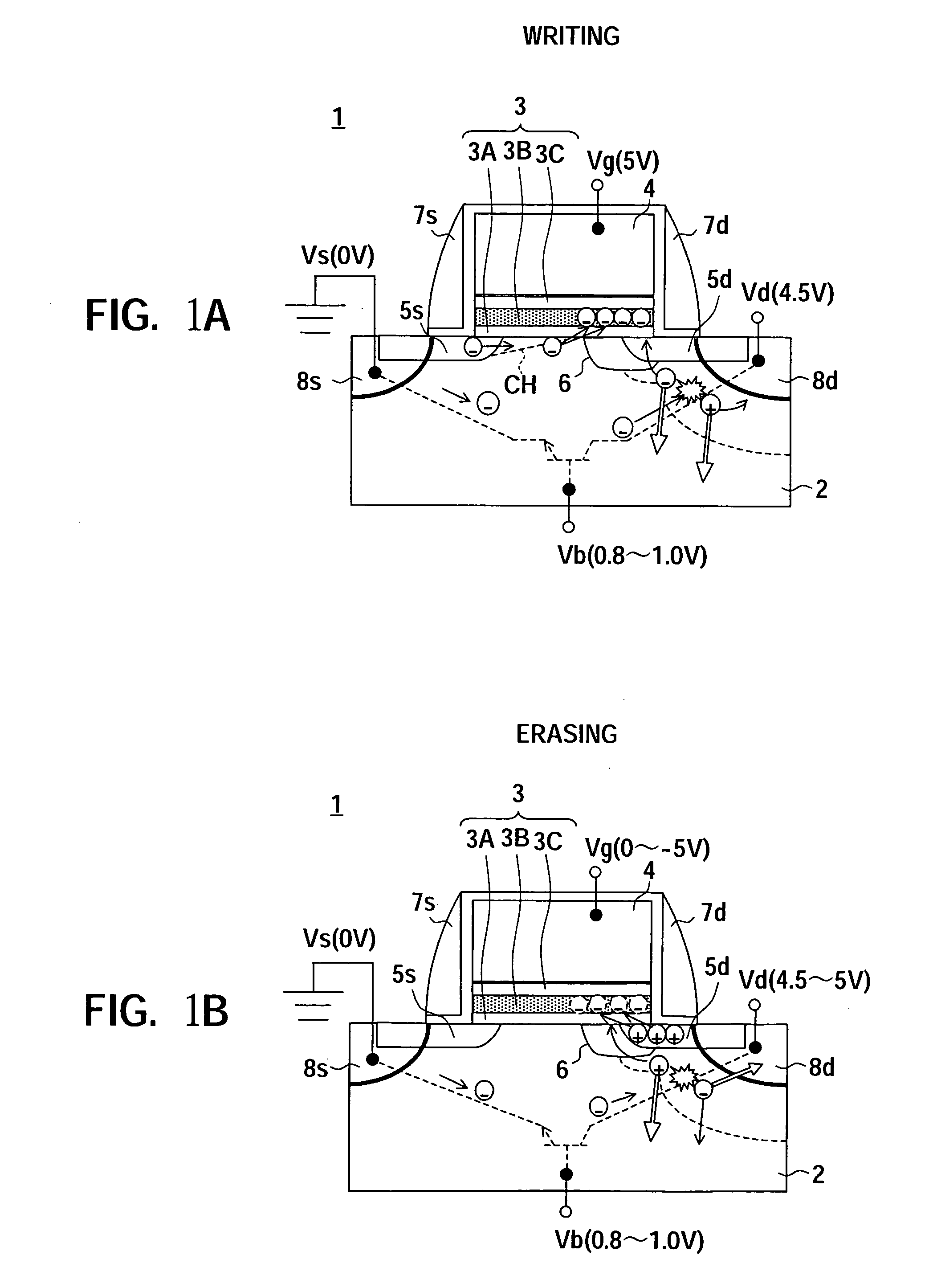
[0040] Below, embodiments of the present invention will be explained with reference to the drawings by taking an example of a flash EEPROM having an N-channel type MONOS transistor.

[0041] Note that the present invention can be applied to memory transistors having a gate electrode configuration except for the MONOS type. For example, the present invention can be widely applied to memory transistors having a gate configuration, such as an FG type, a so-called MNOS (metal-nitride-oxide-semiconductor) type, and a nanocrystal type wherein conductive fine particles are buried in a stacked insulation film. Also, the present invention is not limited to the N-channel type and can be applied to a P-channel type. In that case, by setting conductive types having inverse polarities to an impurity and channel and switching polarities of voltages of a source region and a drain region as will be explained below, an explanation below may be applied analogically.

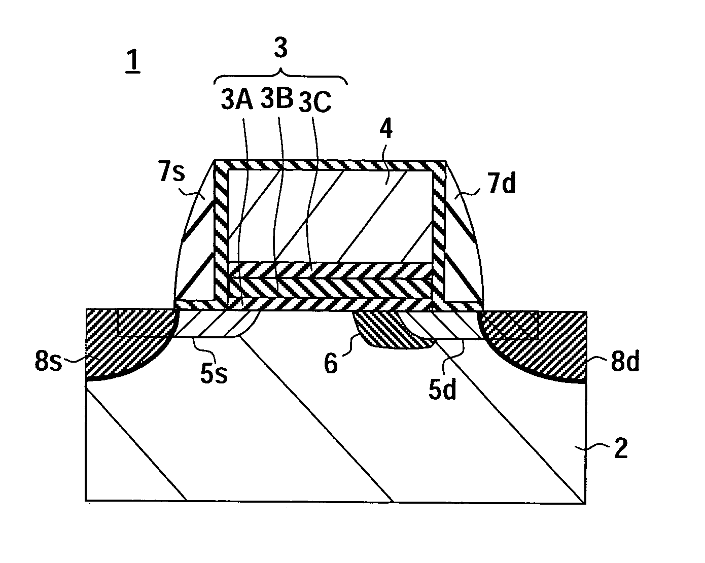
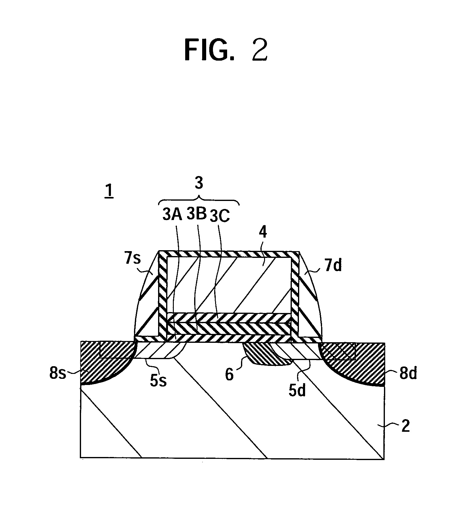
[0042]FIG. 2 is a sectional view of ...


PUM

PropertyMeasurementUnit
Electric chargeaaaaaaaaaa
Electric potential / voltageaaaaaaaaaa
Efficiencyaaaaaaaaaa

Abstract

A charge injection method for improve efficiency of generating hot carrier, wherein, for example, electrons are injected at writing and holes are injected at erasing to a charge storage layer of a memory transistor. A positive voltage is applied to the drain region by using a voltage of the source region as a reference, and a voltage having a polarity in accordance with charges to be injected is applied to a gate electrode. A voltage having a voltage value between a source voltage and a drain voltage for turning on a diode made by an N-type source region and a P-type body region is applied to the body region. Then a parasitic bipolar transistor turns on, consequently, impact ionization arises on the drain side and an injection charge amount increases.

Description

BACKGROUND OF THE INVENTION [0001] 1. Field of the Invention [0002] The present invention relates to a charge injection method of a nonvolatile semiconductor memory device (flash EEPROM) by applying different voltages to a source region and a drain region, a nonvolatile semiconductor memory and an electronic apparatus incorporating the same. [0003] 2. Description of the Related Art [0004] A flash EEPROM as a kind of nonvolatile memories stores data in accordance with a charge storage state of a charge storage layer. As a flash EEPROM, there is a device having a gate structure wherein charges accumulated in a charge storage layer are made by conductive polysilicon (FG type) and that having a gate structure wherein conductivity of the charge storage layer is extremely low as in a typical MONOS (metal-oxide-nitride-oxide-semiconductor) type. In the FG type, electrons are injected, for example, from a whole surface of a channel to tunnel through the gate oxide film, so that the electron...

Claims


Application Information

Patent Timeline
IPC IPC(8): H01L21/8247G11C16/04H01L27/115H01L29/76H01L29/788H01L29/792
CPCG11C16/10H01L21/28282H01L29/872H01L27/11568H01L29/0891H01L27/11565H01L29/40117H10B43/10H10B43/30
Inventor MORI, HIDEKI
Owner SONY CORP
Why Eureka
Try Eureka