IMPATT diodes

a technology of impatt diodes and avalanche, which is applied in the direction of semiconductor/solid-state device manufacturing, semiconductor devices, electrical apparatus, etc., can solve the problems of impatt diodes being noisy and sensitive to operating conditions, and affecting the efficiency of semiconductor devices

Inactive Publication Date: 2004-08-10
CHEMTRON RES
View PDF4 Cites 30 Cited by
  • Summary
  • Abstract
  • Description
  • Claims
  • Application Information

AI Technical Summary

Problems solved by technology

However, IMPATT diodes are noisy and sensitive to operating conditions.
The noise in an IMPATT diode arises mainly from the statistical nature of the generation rates of electron-hole pairs at and above the breakdown voltage.
However, these conditions conflict with conditions favouring high power output and efficiency.
This degrades efficiency as a significant proportion of the generated tunnel current undergoes little or no avalanche multiplication.
Most of the noise associated with a conventional IMPATT diode occurs due to the statistical nature of the generation of electron-hole pairs during the part of the positive half cycle of the oscillating voltage when the voltage is above the threshold breakdown voltage.

Method used


Image

  • IMPATT diodes
  • IMPATT diodes
  • IMPATT diodes

Examples


Embodiment Construction

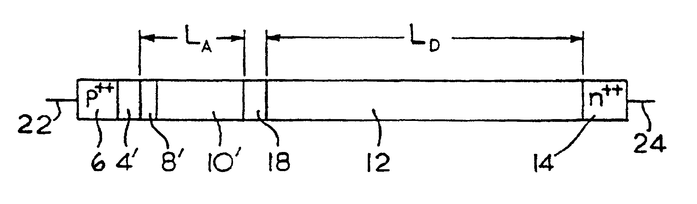
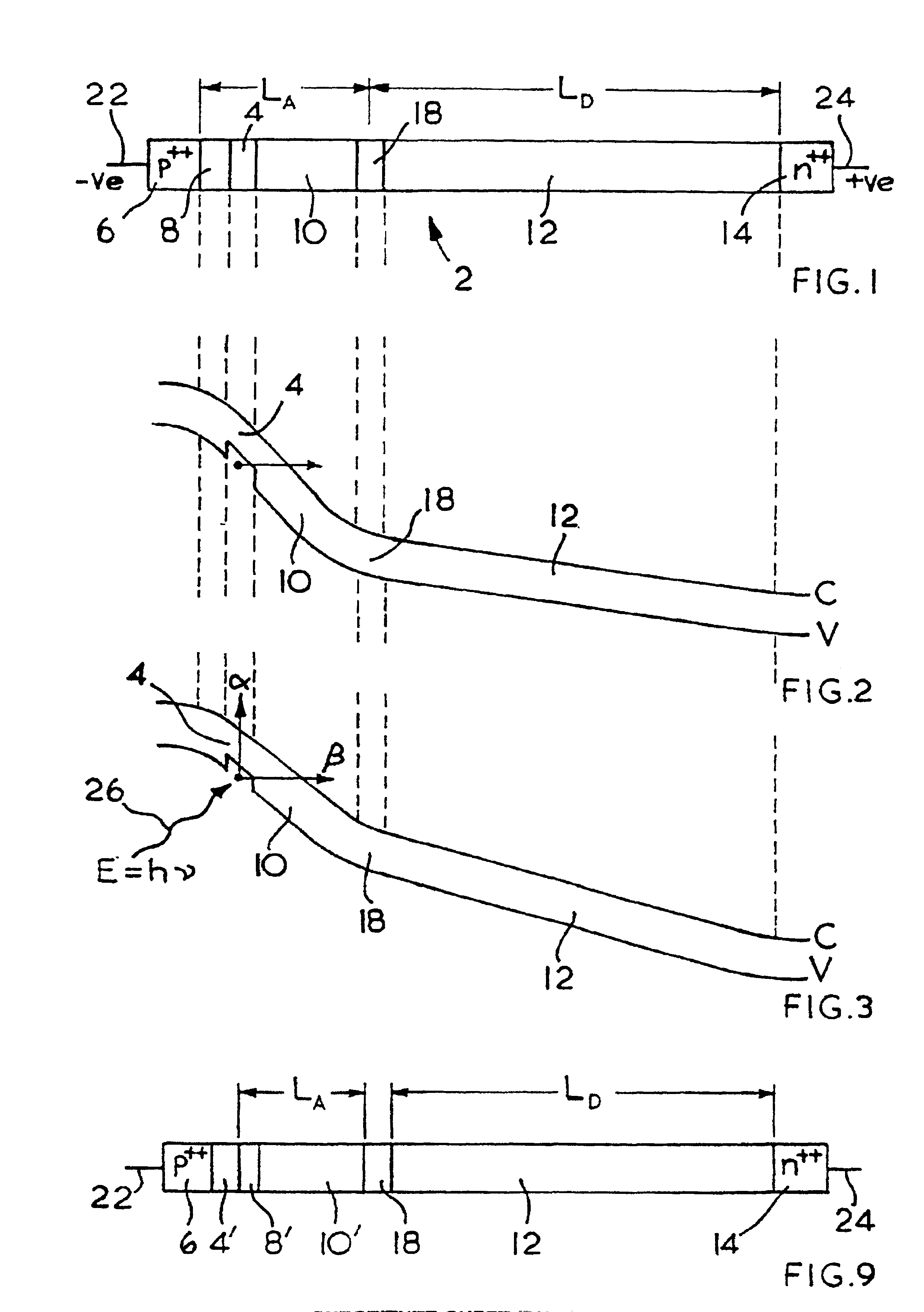
The IMPATT diode (2) shown in FIG. 1 is a lo-hi-lo type IMPATT diode, having a heavily doped p.sup.++ contact region (6), low doped semiconductor regions (8), (10) and (12) and a heavily doped n.sup.++ contact region (14). However, according to the present invention a narrow band gap region (4) is located between the low doped region (8) and the low doped region (10).

The material compositions, layer thickneses and doping used in the IMPATT diode (2) is selected to generate a desired level of tunnel current at the peak reverse bias voltage applied to the diode (2).

The narrow bangap region (4) makes it easier for electrons to tunnel from the valence band (V) to the conduction band (C) and is effective to inject electrons into the conduction band of the wide bandgap region (10) in a predictable manner. This is shown by the arrow in FIG. 2. The electrons injected into the wider bandgap region (10) then undergo avalanche multiplication in the avalanche region (10).

An n-type doping spike ...


PUM


Abstract

The present invention relates to an impact ionisation avalanche transit time (IMPATT) diode device comprising an avalanche region and a drift region, wherein at least one narrow bandgap region, with a bandgap narrower than the bandgap in the avalanche region, is located adjacent to or within the avalanche region in order to generate within the narrow bandgap region a tunnel current which is injected into the avalanche region. This improves the predictability with which a current can be injected into the avalanche region and enables a relatively narrow pulse of current to be injected into the avalanche region in order to enable a relatively noise free avalanche multiplication. The narrow bandgap region may be located between a heavily doped contact region and the avalanche region and is preferably arranged to generate a tunnel current at the peak reverse bias applied to the diode.

Description

1. Field of the InventionThe present invention relates to semiconductor avalanche diodes, and in particular to IMPATT (impact ionisation avalanche transit time) diodes.2. Discussion of Prior ArtIMPATT diodes employ the impact-ionisation and transit time properties of semiconductor structures to produce negative resistance at microwave frequencies. An IMPATT diode consists of heavily doped n.sup.++ and p.sup.++ contact regions separated by a depleted region with a doping m profile designed to produce an avalanche region and a drift region. The doping profile is designed to produce an avalanche region with a high electric field, sufficient to generate high multiplication levels by impact ionisation. The doping profile is designed to produce a drift region with an electric field sufficiently high to achieve carrier velocity saturation but sufficiently low to avoid impact ionisation.A common example of an IMPATT diode has a lo-hi-lo doping profile in which the p.sup.++ contact region is...

Claims


Application Information

Patent Timeline
Patent Type & Authority Patents(United States)
IPC IPC(8): H01L29/66H01L29/864
CPCH01L29/864
Inventor HERBERT, DAVID CDAVIS, ROBERT G
Owner CHEMTRON RES
Why Eureka
Try Eureka