Nonvolatile memory and manufacturing method thereof

a technology of nonvolatile memory and manufacturing method, which is applied in the direction of instruments, semiconductor devices, electrical apparatus, etc., can solve the problems of increase in manufacturing steps, and difficulty in miniaturization and slow write and read speed, so as to achieve the effect of easy impact ionization

Inactive Publication Date: 2003-06-12
SEMICON ENERGY LAB CO LTD
View PDF0 Cites 32 Cited by
  • Summary
  • Abstract
  • Description
  • Claims
  • Application Information

AI Technical Summary

Benefits of technology

[0013] The semiconductor active layer of the memory TFT may have such thickness that impact ionization occurs more easily than that of the switching TFT.
[0019] The semiconductor active layer of the memory TFP may have such thickness that impact ionization occurs more easily than that of the switching TFT.
[0025] The first and second thicknesses may be so set that impact ionization occurs more easily in the first crystalline silicon film than in the second crystalline silicon film.

Problems solved by technology

Although the magnetic disk is one of storage devices having the largest storage capacity among those used for semiconductor devices, it has disadvantages of difficulty in miniaturization and slow write and read speeds.
Therefore, when such a semiconductor nonvolatile memory is mounted on a semiconductor device, the number of manufacturing steps increases and a large-sized package is an obstacle to miniaturization of the semiconductor device.

Method used


Image

  • Nonvolatile memory and manufacturing method thereof
  • Nonvolatile memory and manufacturing method thereof
  • Nonvolatile memory and manufacturing method thereof

Examples


embodiment 1

[0042] This embodiment is directed to a nonvolatile memory formed on an insulative substrate, particularly an EEPROM. An EEPROM according to this embodiment is formed on an insulative substrate so as to be integral with its peripheral circuits such as a driver circuit.

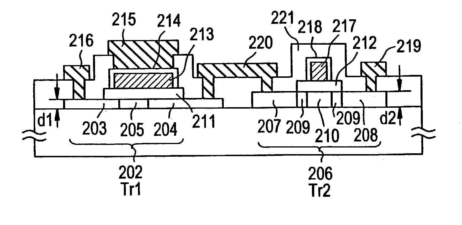
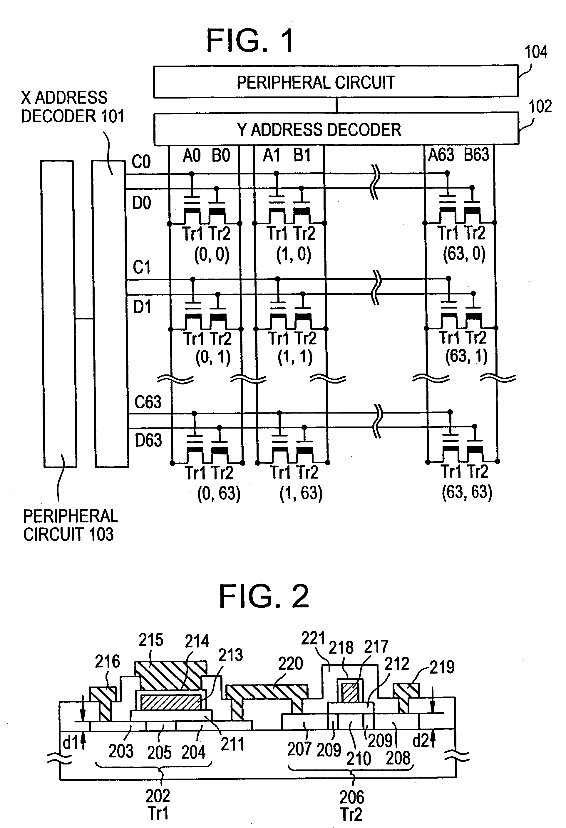
[0043] FIG. 1 is a circuit diagram of a 4-kilobit EEPROM according to this embodiment. As shown in FIG. 1, the 4-kilobit EEPROM according to this embodiment is composed of a plurality of electrically erasable memory elements Tr1, a plurality of switching elements Tr2, X and Y address decoders 101 and 102, and other peripheral circuits 103 and 104. The peripheral circuits 103 and 104 include an address buffer circuit and a control logic circuit and are provided when necessary. Each memory element (storage element) Tr1, which stores bit information in FIG. 1, is a p-channel nonvolatile memory element having a floating gate. Each switching element Tr2 is an n-channel switching element.

[0044] The drain electrodes of two TF...

embodiment 2

[0127] Embodiment 2

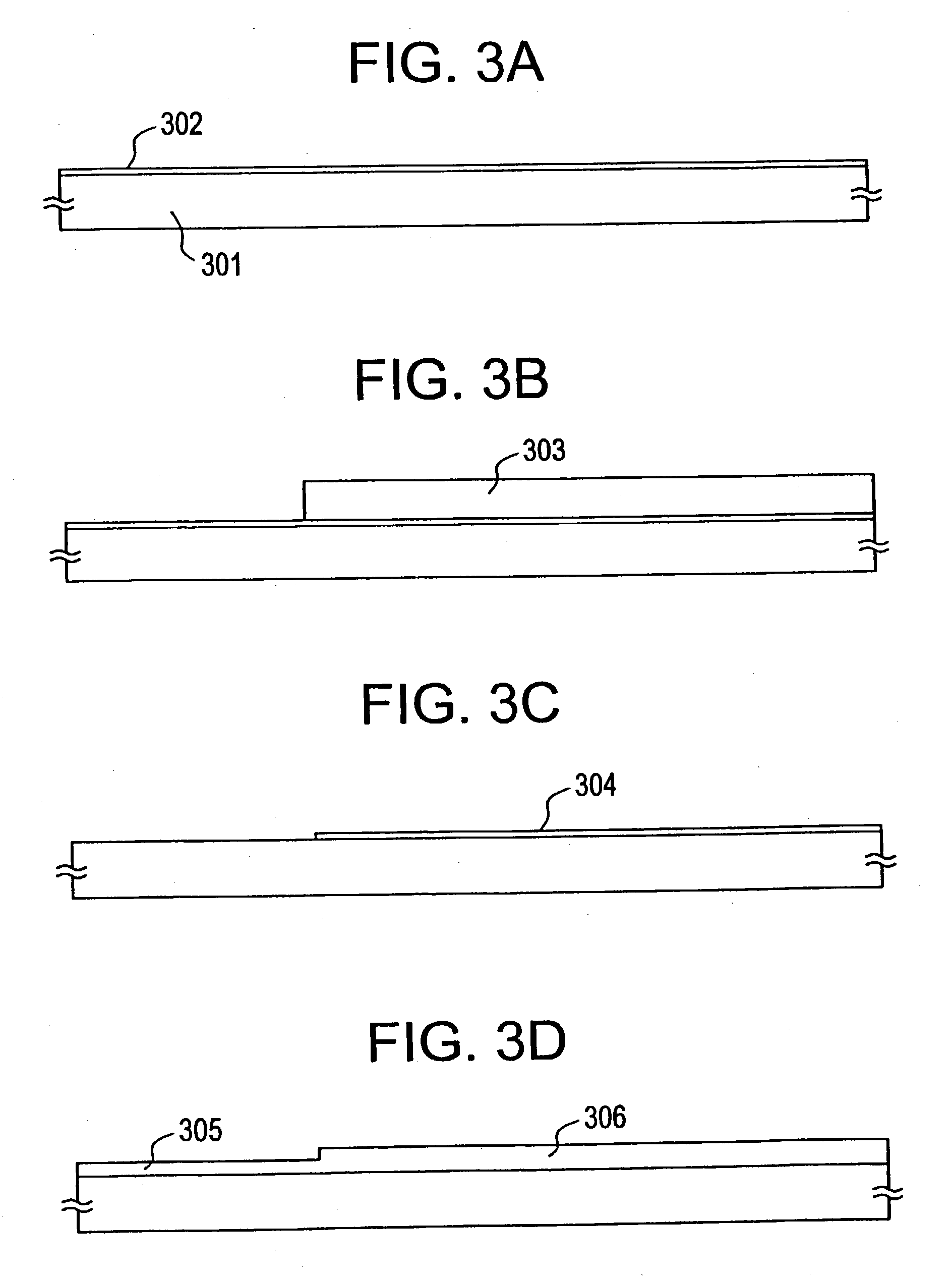
[0128] According to this embodiment, first, an inexpensive, low-grade quartz substrate is prepared. Then, the quartz substrate is polished into an ideal state (average height difference of asperities: within 5 nm, typically within 3 nm, preferably within 2 nm) by CMP (chemical mechanical polishing) or the like.

[0129] In this manner, by subjecting it to polishing, even an inexpensive quartz substrate can be used as an insulative substrate that is superior in flatness. Since a quartz substrate provides a very dense underlying member, the interface between the underlying member and a semiconductor thin film is made highly stable. With an additional advantage that there is almost no contaminative influence from the substrate, this embodiment is very useful.

embodiment 3

[0130] Embodiment 3

[0131] In the first embodiment, a halogen element is used in the step of gettering the catalyst element for accelerating crystallization of silicon. In the invention, the element of phosphorus can also be used in the catalyst element gettering step (this embodiment). The other steps are the same as in the first embodiment.

[0132] Where the element of phosphorus is used, phosphorus may be added to regions other than regions to become active layers and a beat treatment may be performed at 400.degree.-1,050.degree. C. (preferably 600.degree.-750.degree. C.) for 1 minute to 20 hours (typically 30 minutes to 3 hours). As a result of the heat treatment, the catalyst element is gettered in the regions where phosphorus is added, whereby the concentration of the catalyst element in the regions to become active layers is reduced to 5.times.10.sup.17 atoms / cm.sup.3 or less.

[0133] After the completion of the gettering step, active layers are formed by using the regions other t...


PUM


Abstract

Memory elements, switching elements, and peripheral circuits to constitute a nonvolatile memory are integrally formed on a substrate by using TFTs. Since semiconductor active layers of memory element TFTs are thinner than those of other TFTs, impact ionization easily occurs in channel regions of the memory element TFTs. This enables low-voltage write / erase operations to be performed on the memory elements, and hence the memory elements are less prone to deteriorate. Therefore, a nonvolatile memory capable of miniaturization can be provided.

Description

[0001] 1. Field of the Invention[0002] The present invention relates to a nonvolatile memory using thin-film transistors that are formed by using the SOI (silicon on insulator) technology and, particularly, to an EEPROM (electrically erasable and programmable read-only memory) that is formed on an insulative substrate so as to be integral with its peripheral circuits such as a driver circuit. The term "silicon" as used above means a silicon single crystal or a silicon semiconductor that is substantially a single crystal.[0003] 2. Description of the Related Art[0004] In recent years, the miniaturization of semiconductor devices have required memories that has high performance and large storage capacity and is small in size. Currently, among various storage devices for semiconductor devices, the magnetic disk and the semiconductor nonvolatile memory manufactured by using bulk silicon are used most frequently.[0005] Although the magnetic disk is one of storage devices having the larges...

Claims


Application Information

Patent Timeline
Patent Type & Authority Applications(United States)
IPC IPC(8): H01L21/336H01L21/8247H01L21/77H01L21/84H01L27/115H01L27/12H01L29/786H01L29/788H01L29/792
CPCG11C16/0433H01L29/7881H01L27/115H01L27/11526H01L27/11529H01L27/11541H01L27/12H01L27/1203H01L27/1233H01L29/66757H01L29/66765H01L29/78621H01L29/78675H01L29/78678H01L27/105H10B41/40H10B41/41H10B41/47H10B69/00
Inventor YAMAZAKI, SHUNPEIKOYAMA, JUNHAYASHI, KEISUKE
Owner SEMICON ENERGY LAB CO LTD
Why Eureka
Try Eureka