Method of optimizing critical path delay in an integrated circuit design

a critical path delay and integrated circuit technology, applied in computer aided design, program control, instruments, etc., can solve the problems of affecting and the importance of interconnect delay becoming increasingly important, and the overall chip performance of the 90 nanometer technology barely meets the previous generation

Active Publication Date: 2007-02-20
BELL SEMICON LLC
View PDF7 Cites 2 Cited by
  • Summary
  • Abstract
  • Description
  • Claims
  • Application Information

AI Technical Summary

Benefits of technology

[0008](c) selecting an optimum interconnect configuration for minimizing path delay in each timing critical net;

Problems solved by technology

In the aggressive scaling used in deep submicron integrated circuit design, the interconnect delay becomes increasingly important.
However, the overall chip performance of the 90 nanometer technology barely meets that of the previous generation, primarily because of the interconnect delay.

Method used


Image

  • Method of optimizing critical path delay in an integrated circuit design
  • Method of optimizing critical path delay in an integrated circuit design
  • Method of optimizing critical path delay in an integrated circuit design

Examples


Embodiment Construction

[0019]Previous methods used in optimizing an integrated circuit design to achieve timing closure do not address directly the structure of the interconnects. As a result, the optimization may not be effective, and often incurs a power consumption penalty.

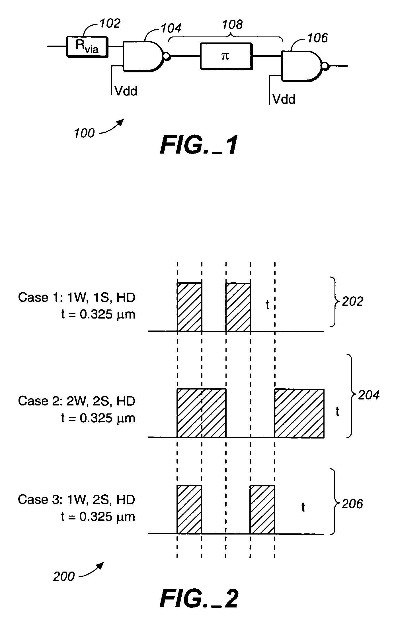
[0020]FIG. 1 illustrates a schematic 100 of an example of a path in a net that requires optimization. Shown in FIG. 1 are a via 102, logic gates 104 and 106, and a critical path 108.

[0021]In FIG. 1, the critical path 108 is identified by a net delay that is 90 percent or more of a clock period. Generally, less than 10 percent of the nets in an integrated circuit design have critical paths due to efficient cell placement criteria. A net that includes a critical path is called a timing critical net.

[0022]FIG. 2 illustrates a graph 200 of three different types of interconnect configuration for the critical path of FIG. 1. Shown in FIG. 2 are a 1-wide, 1-space interconnect configuration 202, a 2-wide, 2-space interconnect configuration 2...


PUM


Abstract

A method and computer program product for optimizing critical path delay in an integrated circuit design include steps of: (a) receiving as input an integrated circuit design; (b) performing a timing / crosstalk analysis to identify each timing critical net in the integrated circuit design; (c) selecting an optimum interconnect configuration for minimizing path delay in each timing critical net; (e) performing a detailed routing that includes the selected optimum interconnect configuration for each timing critical net; and (f) generating as output the detailed routing.

Description

BACKGROUND OF THE INVENTION[0001]1. Field of the Invention[0002]The present invention is directed to the design and manufacture of integrated circuits. More specifically, but without limitation thereto, the present invention is directed to selecting an optimum interconnect configuration for a critical path in an integrated circuit design.[0003]2. Description of Related Art[0004]In the aggressive scaling used in deep submicron integrated circuit design, the interconnect delay becomes increasingly important. For example, a transistor in 90 nanometer technology is about 40 percent faster than that in 130 nanometer technology of the previous generation. However, the overall chip performance of the 90 nanometer technology barely meets that of the previous generation, primarily because of the interconnect delay. In 90 nanometer integrated circuit technology and deeper, the interconnect delay plays an increasingly important role in timing closure of the integrated circuit design.SUMMARY OF...

Claims


Application Information

Patent Timeline
Patent Type & Authority Patents(United States)
IPC IPC(8): G06F17/50
CPCG06F17/5031G06F17/505G06F17/5036G06F30/3312G06F30/327G06F30/367G06F2119/12
Inventor MBOUOMBOUO, BENJAMINLI, WEIDANAHRENS, DANA
Owner BELL SEMICON LLC
Why Eureka
Try Eureka