Apparatus for cooling semiconductor devices attached to a printed circuit board

a technology of printed circuit board and semiconductor device, which is applied in the direction of electrical apparatus, electrical apparatus contruction details, lighting and heating apparatus, etc., can solve the problems of reduced reliability of semiconductor device, difficult to attach radiating fin b>102/b> to ic b>104/b>, and difficult wiring pattern on printed circuit board. , to achieve the effect of less manufacturing process, less parts, and less weigh

Active Publication Date: 2007-03-06
HARMAN BECKER AUTOMOTIVE SYST
View PDF13 Cites 33 Cited by
  • Summary
  • Abstract
  • Description
  • Claims
  • Application Information

AI Technical Summary

Benefits of technology

[0014]A positive cooling effect is achieved regardless of mounting conditions and the position of the semiconductor device on the cooling plate. Further, the manufacturing process is less costly, less parts are needed, and less weight and less height are required.

Problems solved by technology

The electric power consumed by a single semiconductor device, especially those with power transistors, has become so large that there are increasing instances where the device becomes heated to the point that reliability of the semiconductor device is decreased.
If the resistance of heat transfer between the surface of the heated element and the surrounding air is low, then the undesirable heat is suitably transferred.
As a result, the wiring pattern on the printed circuit board is also subject to restriction.
Second, the technique used for attaching the radiating fin 102 to the IC 104 is often problematic.
However, the conventional apparatus shown in FIG. 2 still exhibits some limitations as, for example, a costly manufacturing process, a relatively large number of specific parts, and unreasonable weight and height in view of the cooling effect achieved.

Method used


Image

  • Apparatus for cooling semiconductor devices attached to a printed circuit board
  • Apparatus for cooling semiconductor devices attached to a printed circuit board
  • Apparatus for cooling semiconductor devices attached to a printed circuit board

Examples


Embodiment Construction

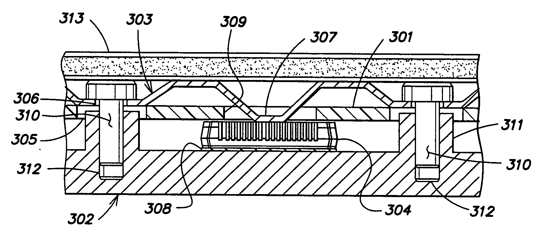
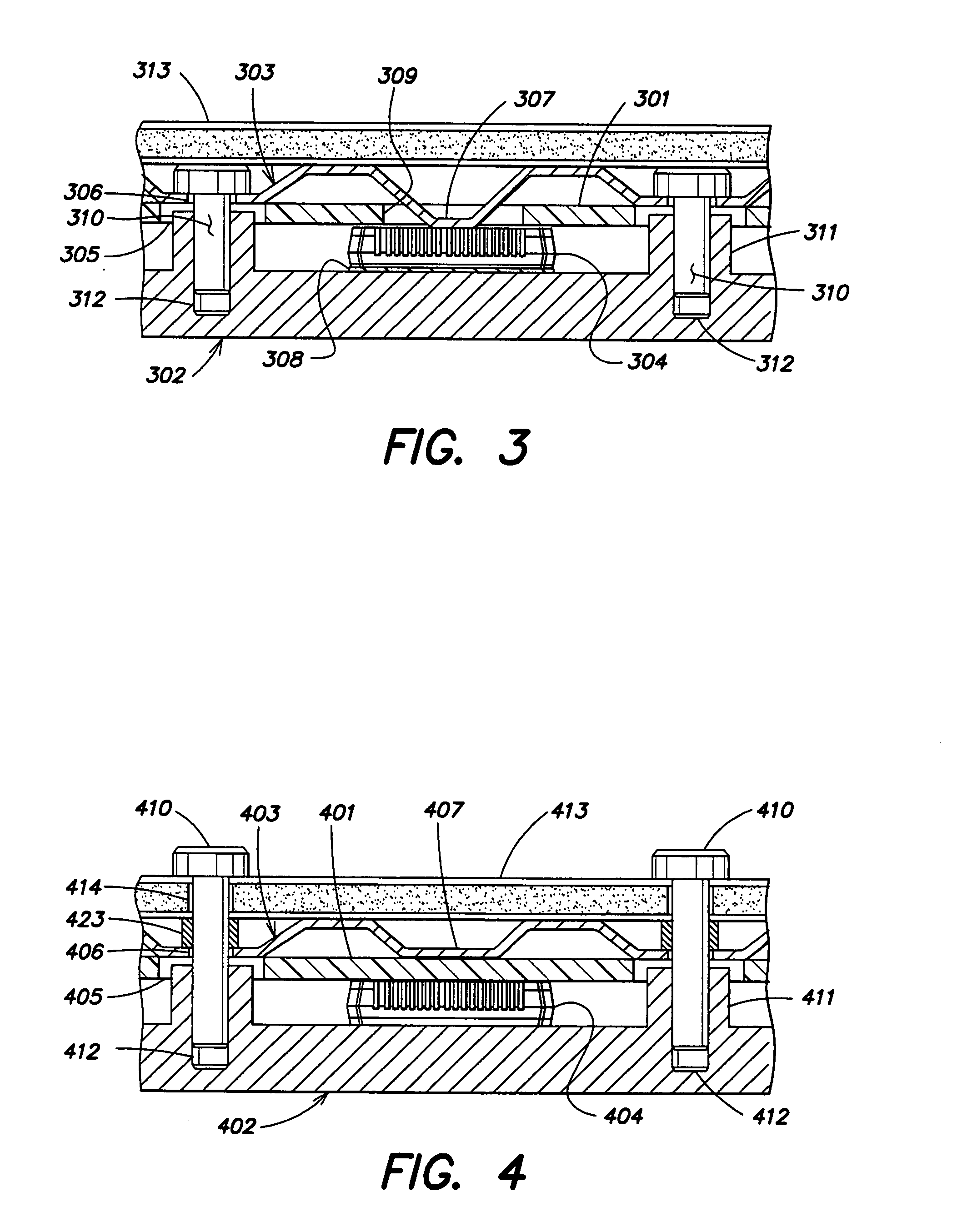
[0024]The present invention provides an apparatus for cooling semiconductor devices attached to a printed circuit board. As shown in FIG. 3, a printed circuit board 301 is sandwiched between a cooling plate 302 and a spring plate 303 (e.g. a leaf spring).

[0025]The printed circuit board 301 is a plate of electrically non-conductive material (e.g., resin plate, ceramic substrate) comprising at least one structured electrically conductive layer (e.g., metallization) for connecting electrical devices such as semiconductor devices mounted on the printed circuit board. The printed circuit board 301 has first and second sides and further comprises a plurality of apertures 305 formed through the first and second sides. The first side of the printed circuit board 301 comprises a semiconductor device 304 (e.g., power amplifier, voltage regulator, or a power switch, et cetera) attached thereto (e.g., by soldering). In FIG. 3 the printed circuit board 301 comprises a further aperture 309 arrang...


PUM


Abstract

An electronic assembly includes a semiconductor device mounted on a printed circuit board, a leaf spring and a cooling plate. A plurality of fasteners pass through co-axial apertures of the leaf spring, the printed circuit board and the cooling plate, such that a contact surface of the leaf spring imparts a force on the semiconductor device to retain the semiconductor device in a thermally conductive position with respect to the cooling plate. A positive cooling effect is achieved regardless of mounting conditions including orientation of the electronic assembly, and the position of the semiconductor device on the cooling plate.

Description

CLAIM OF PRIORITY[0001]This patent application claims priority to European Application EP 03 018 046.7 filed on Aug. 7, 2003.[0002]1. Field of the Invention[0003]The present invention relates to the field of cooling semiconductor devices, and in particular to the field of devices for cooling semiconductor devices attached to a printed circuit board.[0004]2. Related Art[0005]The electric power consumed by a single semiconductor device, especially those with power transistors, has become so large that there are increasing instances where the device becomes heated to the point that reliability of the semiconductor device is decreased. The heat radiation to cool the semiconductor device relies upon heat transfer from the surface of the heated portion to the surrounding air. If the resistance of heat transfer between the surface of the heated element and the surrounding air is low, then the undesirable heat is suitably transferred. Therefore, by lowering the heat transfer resistance to t...

Claims


Application Information

Patent Timeline
Patent Type & Authority Patents(United States)
IPC IPC(8): H05K7/20H01L23/40H01L23/433
CPCH01L23/4006H01L23/433H01L2924/0002H01L2924/00
Inventor SCHMIDBERGER, STEFAN
Owner HARMAN BECKER AUTOMOTIVE SYST
Why Eureka
Try Eureka