Semiconductor memory device and method for manufacturing same

a semiconductor memory and memory device technology, applied in static storage, digital storage, instruments, etc., can solve the problems of increased chip cost, inability to repair this semiconductor memory device,

Inactive Publication Date: 2007-03-06
LONGITUDE LICENSING LTD
View PDF6 Cites 78 Cited by
  • Summary
  • Abstract
  • Description
  • Claims
  • Application Information

AI Technical Summary

Benefits of technology

[0026]The seventh aspect of the present invention is a method for manufacturing a semiconductor memory comprising the steps of: repairing a failed cell by using either row redundancy or column redundancy; and repairing remaining failed cells that cannot be repaired by the first repairing step by increasing the number of refreshes of the failed cell greater than that of normal cell.

Problems solved by technology

In the process of repairing failed cells in the conventional semiconductor memory device configured as noted above, there is the problem that in the case in which all the redundant circuits are quickly used up in one segment, even if there are remaining usable redundant circuits in other segments, because the above-noted segment has used up all its redundant circuits, it becomes impossible to repair this semiconductor memory device.
In a method of repairing such a semiconductor memory device, there is the additional problem of increased chip cost, caused by the need to provide a greater number of redundant cells.

Method used


Image

  • Semiconductor memory device and method for manufacturing same
  • Semiconductor memory device and method for manufacturing same
  • Semiconductor memory device and method for manufacturing same

Examples


first embodiment

The First Embodiment

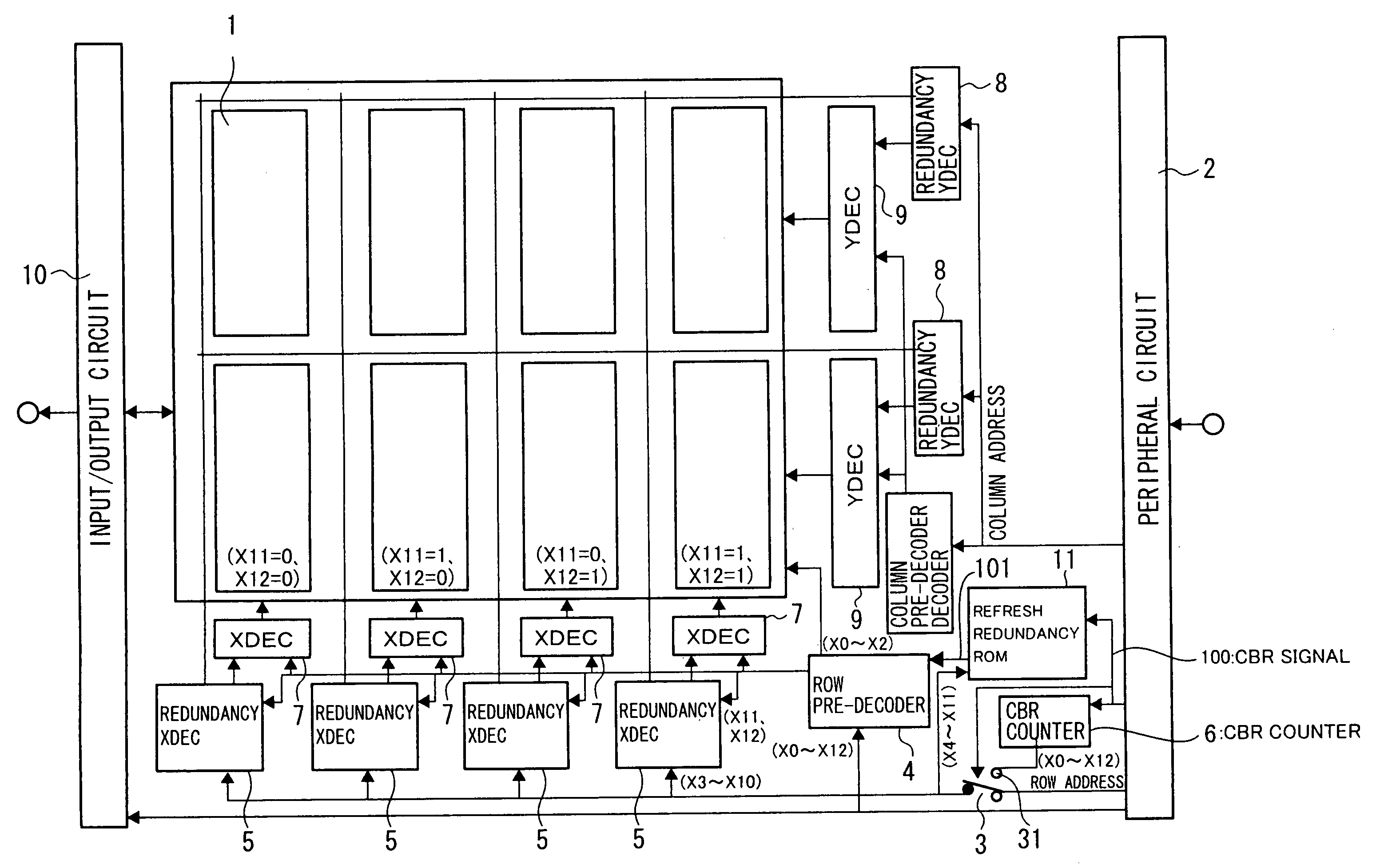
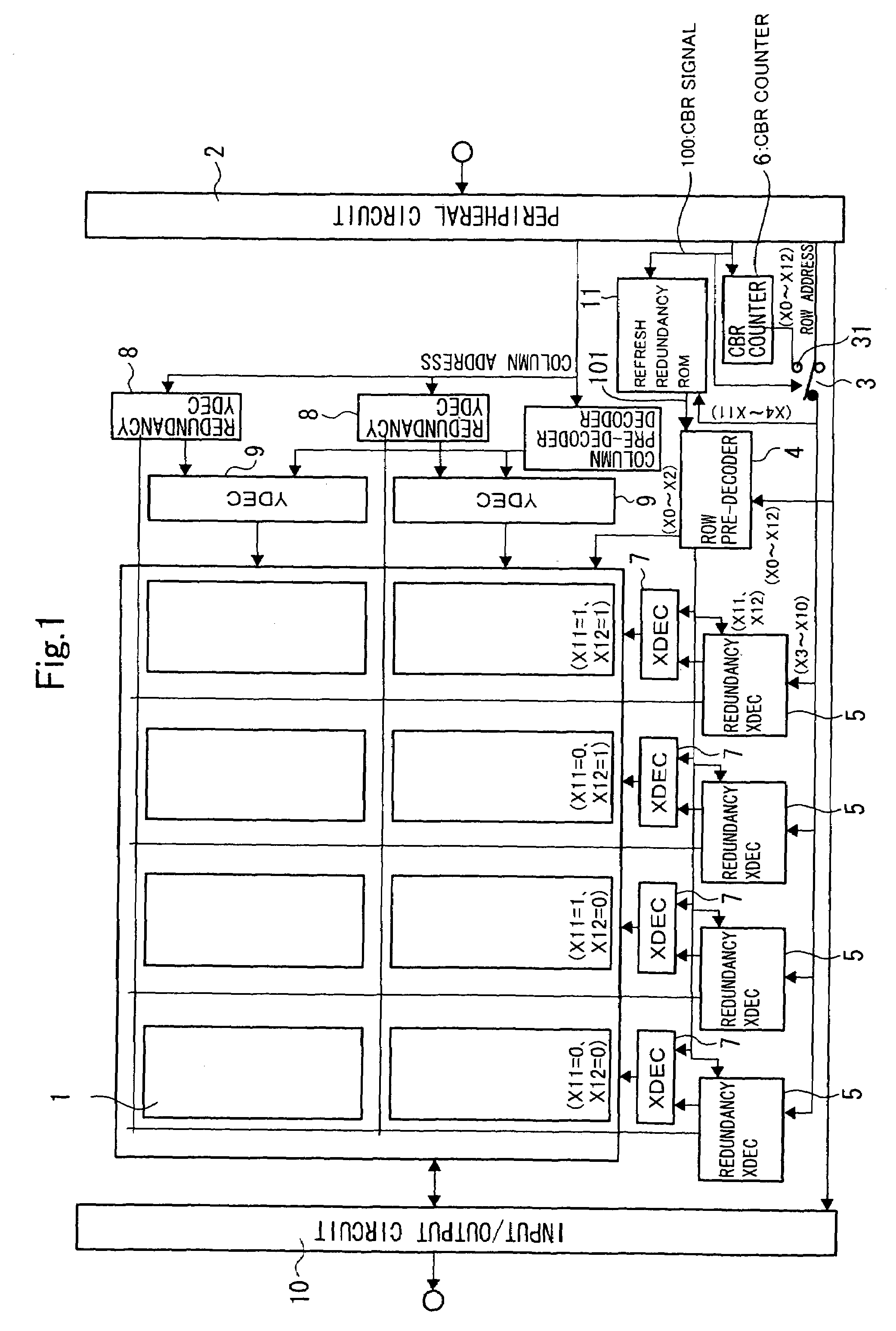
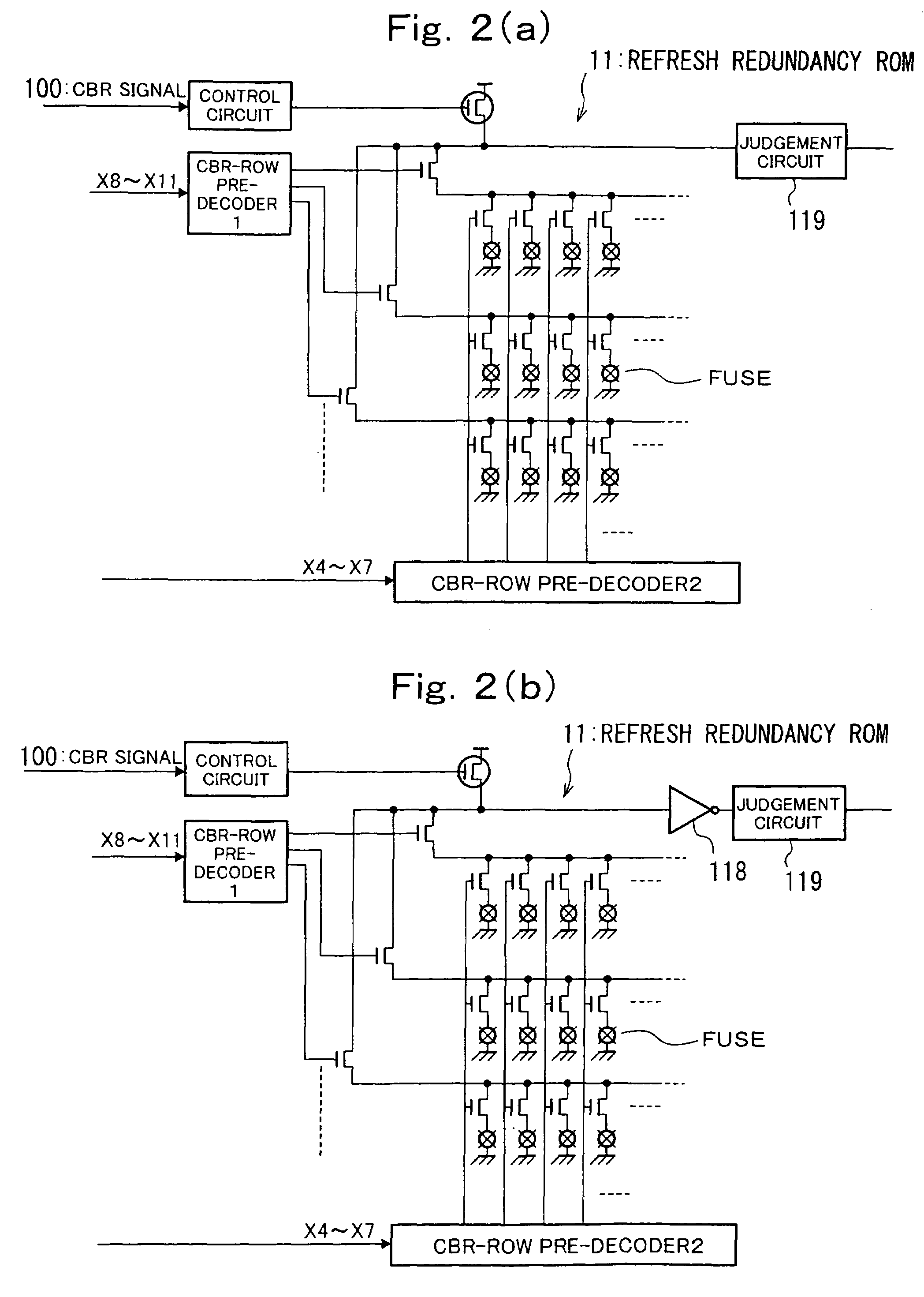
[0048]FIG. 1 to FIG. 3 are drawings showing the first embodiment of the present invention, FIG. 1 being a block diagram showing the configuration of the first embodiment, FIG. 2 being a drawing showing the detailed configuration of the refresh redundancy ROM, and FIG. 3 being a timing diagram showing the operation of the first embodiment.

[0049]The difference between the circuit blocks between FIG. 1 and FIG. 11 is that the first embodiment includes the refresh redundancy ROM 11. Other aspects of the configuration, however, are the same as the past example shown in FIG. 11. Accordingly, the same reference numerals have been applied to corresponding parts, which are not described in detail herein.

[0050]FIG. 2(a) is a drawing showing the configuration of the refresh redundancy ROM 11 in the first embodiment which is formed by MOS switches and fuses arranged in the form of a matrix and a judgment circuit 119, wherein redundancy cell addresses are programmed so that f...

second embodiment

The Second Embodiment

[0059]The second embodiment of the present invention is described below with reference made to FIG. 2, FIG. 4 and FIG. 5, FIG. 4 being a block diagram showing the second embodiment, and FIG. 5 being a timing diagram showing the operation of the second embodiment.

[0060]The second embodiment differs from the first embodiment in that a D-type flip-flop 12 is provided, which latches the output of the refresh redundancy ROM 11.

[0061]In this case, it is also possible to use another type of holding circuit in place of the D-type flip-flop 12, as long as it enables the latching of the output of the refresh redundancy ROM 11.

[0062]In the second embodiment, as shown in FIG. 5, when the CBR signal 203 of the immediately previous REF command 201 is reset, the CBR counter 6 counts up, a refresh redundancy judgment being made in advance at this address and, if there is coincidence, a coincidence pulse 204 is output from the refresh redundancy ROM 11, this data being held in t...

third embodiment

The Third Embodiment

[0069]FIG. 6 is a timing diagram showing the operation of the third embodiment.

[0070]The semiconductor memory device according to the third embodiment provided with a D-type flip-flop 12 that latches the output of the refresh redundancy ROM 11.

[0071]The third embodiment differs from the second embodiment in that the address programmed into the refresh redundancy ROM 11 is the address immediately before the address of the cell which is to be repaired by “refresh repair” of the present invention.

[0072]Specifically, in the case of FIG. 9, since the address of the failed cell is CA5Bh, the programmed address is CA5Ah.

[0073]That is, in the third embodiment, when the REF command 201 is output, a judgment is made as to whether a memory cell at the address corresponding to the next REF command 202 is to be repaired by “refresh repair” and a coincidence signal 204A is latched by the D-type flip-flop 12. In this embodiment, when the REF command 202 for refreshing a cell is...


PUM


Abstract

At first, failed cells are repaired using row redundancy or column redundancy as done in the past and then, for the remaining failed cells that cannot be repaired by row or column redundancy, by increasing the number of refreshes greater than that of normal cells, it is possible to repair more failed cells.

Description

BACKGROUND OF THE INVENTION[0001]1. Field of the Invention[0002]The present invention relates to a semiconductor memory device and to a method for manufacturing same. More particularly, it relates to a semiconductor memory device having redundant cells, in which failed cells are repaired using row redundancy or column redundancy of the prior art, and further in which remaining failed cells not repairable using row redundancy or column redundancy are repaired by increasing the number of refreshes thereby repairing these cells and increasing manufacturing yield.[0003]2. Related Art[0004]FIG. 11 of the accompanying drawings is a conventional block diagram showing the configuration of a semiconductor memory device.[0005]In FIG. 11, the reference numeral 1 denotes a memory array, 2 is a peripheral circuit, 3 is a switch, 4 is a row pre-decoder, 5 is a redundant X decoder, and 6 is a CBR counter, this semiconductor memory device in FIG. 11 is provided with a plurality of separated segment...

Claims


Application Information

Patent Timeline
Patent Type & Authority Patents(United States)
IPC IPC(8): G11C7/00G11C29/04G11C11/406G11C29/00
CPCG11C11/406G11C29/78
Inventor KOSHIKAWA, YASUJI
Owner LONGITUDE LICENSING LTD
Why Eureka
Try Eureka