
Calibrated PLL for wide band communication semiconductor integrated polar loop transmitter

a wide band communication, integrated polar loop technology, applied in the direction of multi-channel communication, digital transmission, modulation, etc., can solve the problem of not achieving a sufficient reduction of the number of components, and achieve the effect of enhancing the accuracy of oscillation frequency, improving evm, and enhancing modulation accuracy

Active Publication Date: 2007-03-06
RENESAS CO CORP
View PDF7 Cites 7 Cited by
  • Summary
  • Abstract
  • Description
  • Claims
  • Application Information

AI Technical Summary

Benefits of technology

"The invention aims to solve the problem of deteriorated performance in the phase control loop and the amplitude control loop of a communication semiconductor integrated circuit (RF IC) that incorporates a transmission oscillator. The RF IC needs to secure the oscillation operation over a wide frequency range and enhance the accuracy of the oscillation frequency. The invention proposes a technique to prevent the deterioration of the EVM and the transmission spectrum, which leads to the attenuation of signal level and increases the leakage of noises into adjacent channels. The invention provides a solution to secure the oscillation operation and enhance the accuracy of the oscillation frequency in the phase control loop and the amplitude control loop of the RF IC."

Problems solved by technology

As the result, the examination discovered the following problems.
But this cannot achieve a sufficient reduction of the number of components.

Method used


Image

  • Calibrated PLL for wide band communication semiconductor integrated polar loop transmitter
  • Calibrated PLL for wide band communication semiconductor integrated polar loop transmitter
  • Calibrated PLL for wide band communication semiconductor integrated polar loop transmitter

Examples


Embodiment Construction

[0046]Next, the embodiment of the invention will be described with the accompanying drawings.

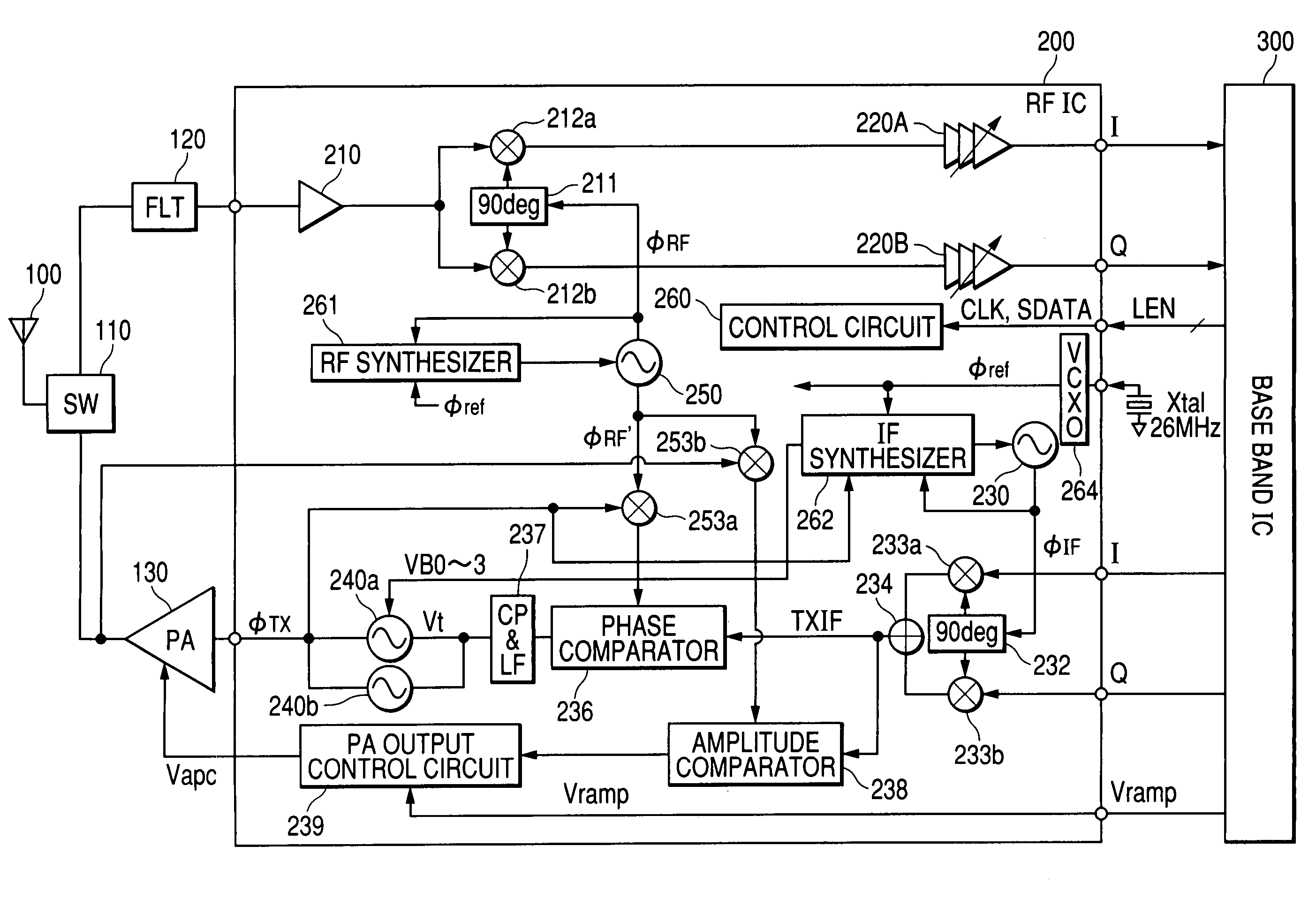
[0047]FIG. 1 is a block diagram that shows one embodiment of a communication semiconductor integrated circuit (RF IC) incorporating a transmission oscillator relating to the invention, and a configuration example of a radio communication system using the RF IC. This embodiment was applied to a radio communication system of the EDGE system that executes the 8-PSK modulation by the so-called polar loop system having the phase control loop and the amplitude control loop.

[0048]The radio communication system shown in FIG. 1 includes an antenna 100 that transmits / receives radio wave signals, a switch 110 that switches the transmission / reception, a band pass filter 120 that removes undesired signals from a reception signal, being made up with a SAW filter and so forth, an RF power amplification circuit (power amplifier) 130 that amplifies a transmission signal, an RF IC 200 that demodulates the rec...


PUM


Abstract

The invention provides a communication semiconductor integrated circuit (RF IC) that, when a transmission oscillator is incorporated into a semiconductor chip, secures the oscillation operation over a wide frequency range, prevents a deterioration of a transmission spectrum, and thereby enhances the accuracy of an oscillation frequency. The integrated circuit corrects a dispersion of the KV characteristic of the transmission oscillator by calibrating a current Icp of the charge pump inside the phase control loop. More in concrete, the integrated circuit measures a KV value Kv of the transmission oscillator, and calibrates the current Icp of the charge pump so that Kv·Icp falls into a predetermined value.

Description

CROSS-REFERENCE TO RELATED APPLICATION[0001]The present application claims priority from Japanese application patent no. JP 2003-323995 filed on Sep. 17, 2003, the content of which is hereby incorporated by reference into this application.BACKGROUND OF THE INVENTION[0002]The present invention relates to a technique effective in an application to incorporating a voltage controlled oscillator (VCO) capable of switching an oscillation frequency into a semiconductor chip, specifically to a technique effective in use for a control loop of a transmission VCO in a high frequency semiconductor integrated circuit that modulates or up-converts a transmission signal, which is used in a radio communication device such as a mobile telephone capable of transmitting and receiving signals of plural bands.[0003]There is a system called the GSM (Global System for Mobile Communication), which is used in the field of the radio communication device (mobile communication device) such as a mobile telephon...

Claims


Application Information

Patent Timeline
Patent Type & Authority Patents(United States)
IPC IPC(8): H04B1/04H03B5/12H03L7/089H03L7/093H03L7/099H03L7/10H03L7/16H04B1/40
CPCH03L7/0898H03L7/099H03L7/16H03B5/1253H03B5/1228H03B5/1215H03B5/1243H04B1/403
Inventor ARAYASHIKI, SATOSHIOOSAWA, HIROTAKAKURAKAMI, NORIYUKIOKASAKA, AKIRAKIMURA, YASUYUKIUOZUMI, TOSHIYAMIYAGAWA, HIROKAZUTANAKA, SATOSHI
Owner RENESAS CO CORP
Learn More