Radiation image conversion panel and preparation method thereof
a technology of conversion panel and radiation image, which is applied in the direction of conversion screen, instruments, nuclear engineering, etc., can solve the problems of deterioration of luminance and sharpness, and reduce contrast, and achieve the effect of lowering contras
- Summary
- Abstract
- Description
- Claims
- Application Information
AI Technical Summary
Benefits of technology
Problems solved by technology
Method used
Image
Examples
example 1
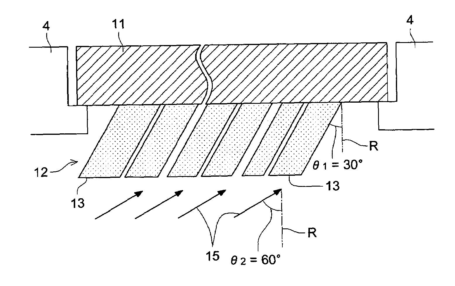
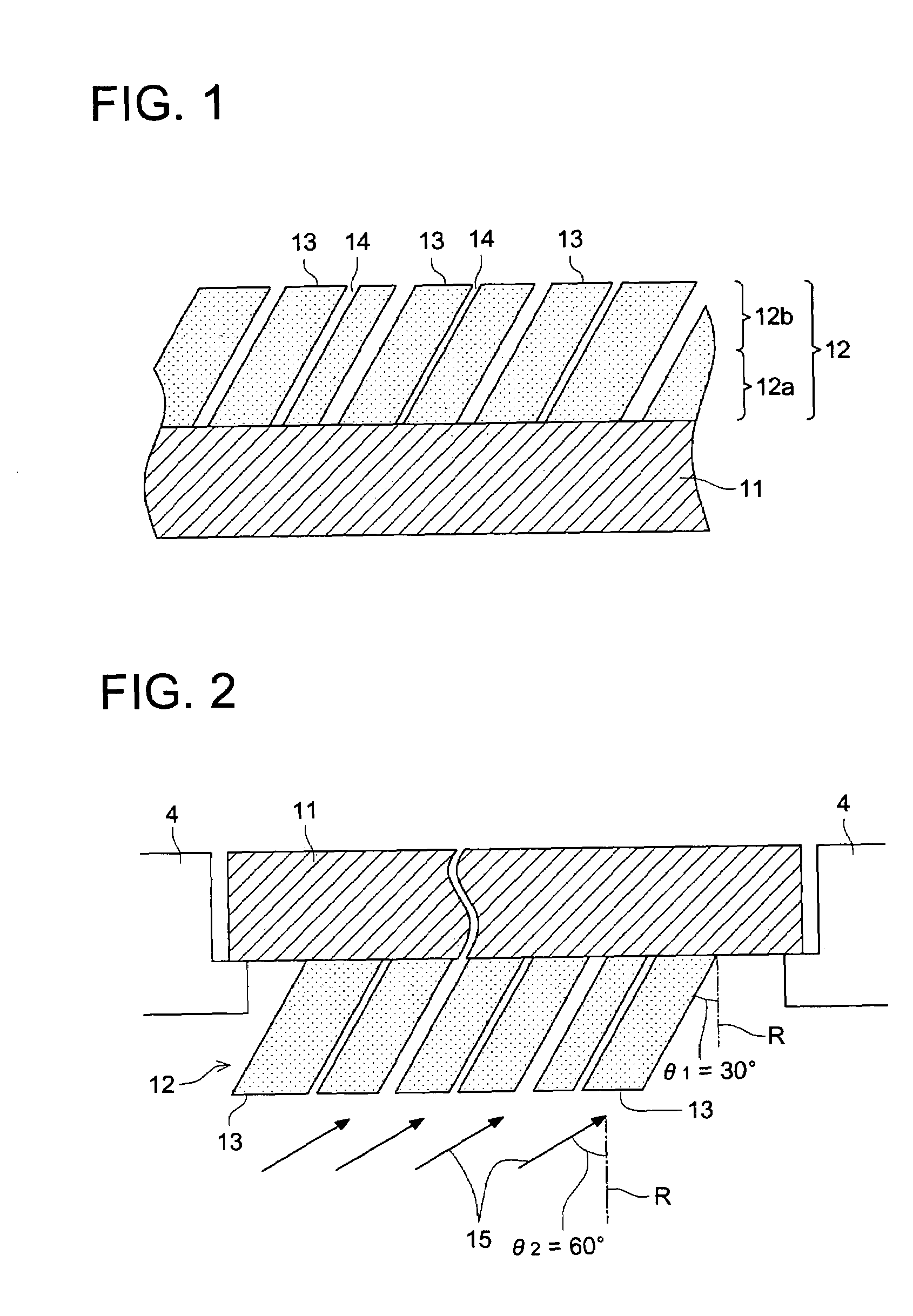
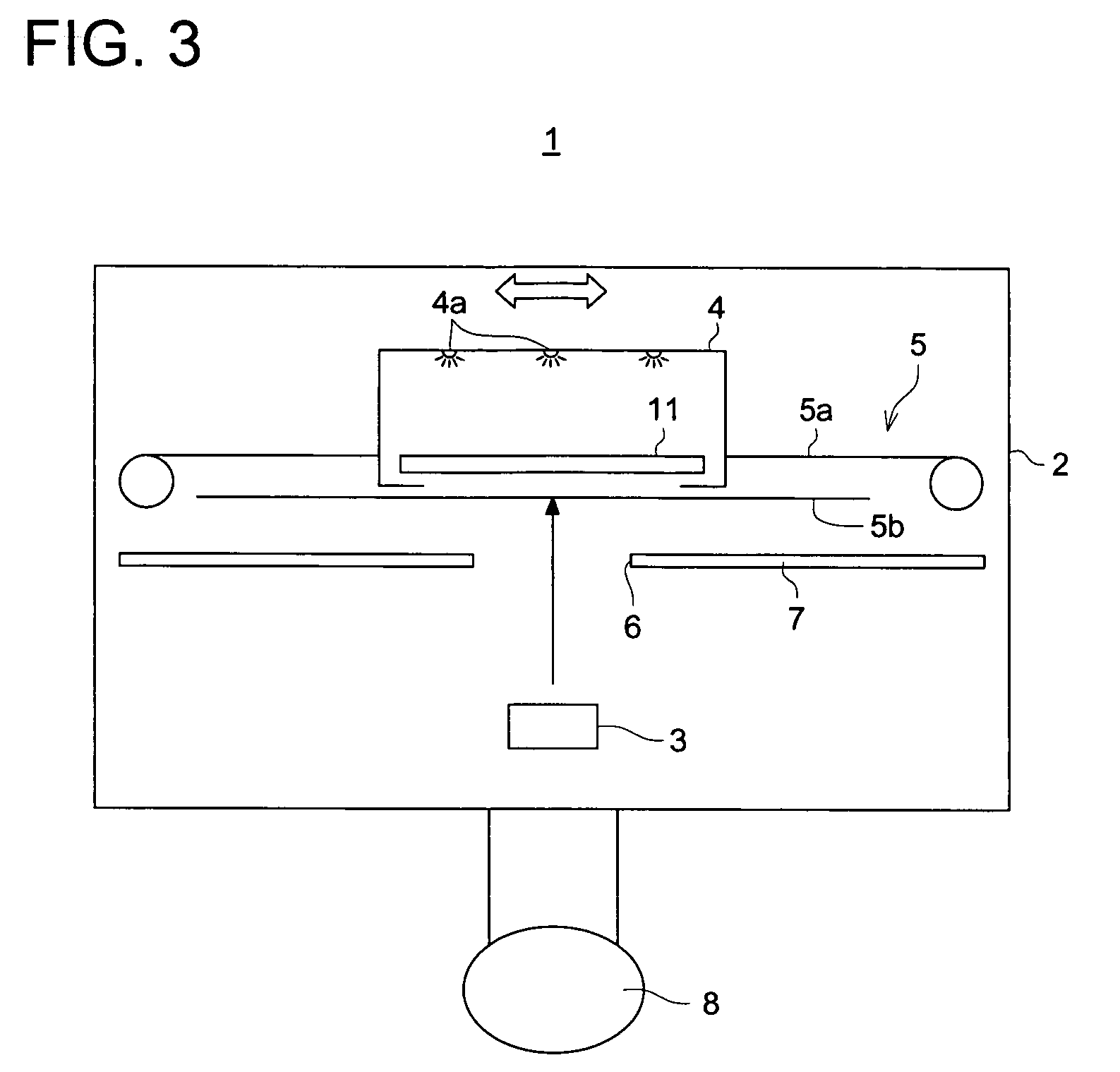
[0049]Using a vacuum deposition apparatus (1) as shown in FIG. 3 (which was set to θ1=5° and θ2=5°, as shown in FIG. 2), a layer of columnar crystal structure which was composed of a parent component (CsBr) of a stimulable phosphor, was formed on a 1 mm thick crystallized glass (produced by Nippon Denki Glass Co.) and subsequently, further thereon, a stimulable phosphor layer composed of a parent component and an activator component (CsBr:0.0002Eu) was formed. In the evaporation apparatus (1), an aluminum shutter plate (7) was used and the distance between a support (11) and the shutter plate (7) was maintained at 60 cm and deposition was carried out while transporting the support (11) in the direction parallel to the surface of the support (11). After evacuating the interior of the deposition apparatus (1), Ar gas was introduced to adjust the vacuum to 1.0×10⁻² Pa and deposition was carried out while maintaining the support (11) at a temperature of 150° C. When a CsBr layer reached...
example 2
[0051]A radiation image conversion panel was prepared similarly to Example 1, except that the thickness of the CsBr:Eu layer was 500 μm. It was proved that the main crystal growth of the stimulable phosphor layer was a (200) plane and the X-ray absorptance was 89%.
example 3
[0052]A radiation image conversion panel was prepared similarly to Example 1, except that the thickness of the CsBr:Eu layer was 800 μm. It was proved that the main crystal growth direction of the stimulable phosphor layer was a (200) plane and the X-ray absorptance was 95%.
PUM
| Property | Measurement | Unit |
|---|---|---|
| thickness | aaaaa | aaaaa |
| thickness | aaaaa | aaaaa |
| thickness | aaaaa | aaaaa |
Abstract
Description
Claims
Application Information


