Lead frame

a lead frame and frame technology, applied in the field of lead frame, can solve the problems of reducing the pitch of the pin, limiting the reduction of the package size, and more complication during fabrication, so as to increase the number of contact members and reduce the pitch of the contact members

Inactive Publication Date: 2007-03-20
INFINEON TECH AG
View PDF9 Cites 68 Cited by
  • Summary
  • Abstract
  • Description
  • Claims
  • Application Information

AI Technical Summary

Benefits of technology

[0006]An advantage of the invention is that by having contact members which extend both towards and away from the first portion, it is possible to increase the number of contact members for a given package size without requiring a decrease in the pitch of the contact members.
[0007]Preferably, the ends of the first and second contact members remote from the main member are substantially co-planar.
[0008]Typically, the first portion may also be co-planar with the remote ends of the first and second contact members.
[0009]Preferably, the first contact members are offset along the main member from the second contact members.
[0010]Typically, the spacing between the first contact members adjacent the main member is greater than the width of the second contact members adjacent to the main member.
[0011]Preferably, the spacing between the second contact members adjacent to the main member is greater than the width of the first contact members adjacent to the main member.

Problems solved by technology

However, the increase in pin count places a limitation on the reduction of the package size, unless the pitch of the pins is reduced.
Reducing the pitch of the pins leads to more complication during fabrication as it requires processes, such as stamping tool fabrication, dambar cut process, testing and surface mount technology to be more accurate.
Therefore, there is a conflict between increasing system integration, which results in a higher pin count, and reducing the size of the integrated circuit package.

Method used


Image

  • Lead frame
  • Lead frame
  • Lead frame

Examples


Embodiment Construction

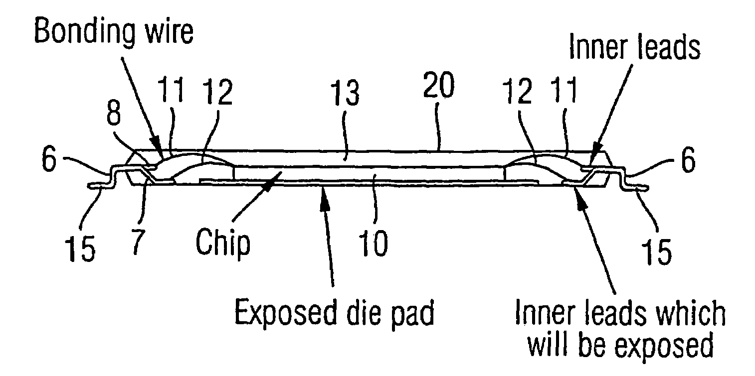
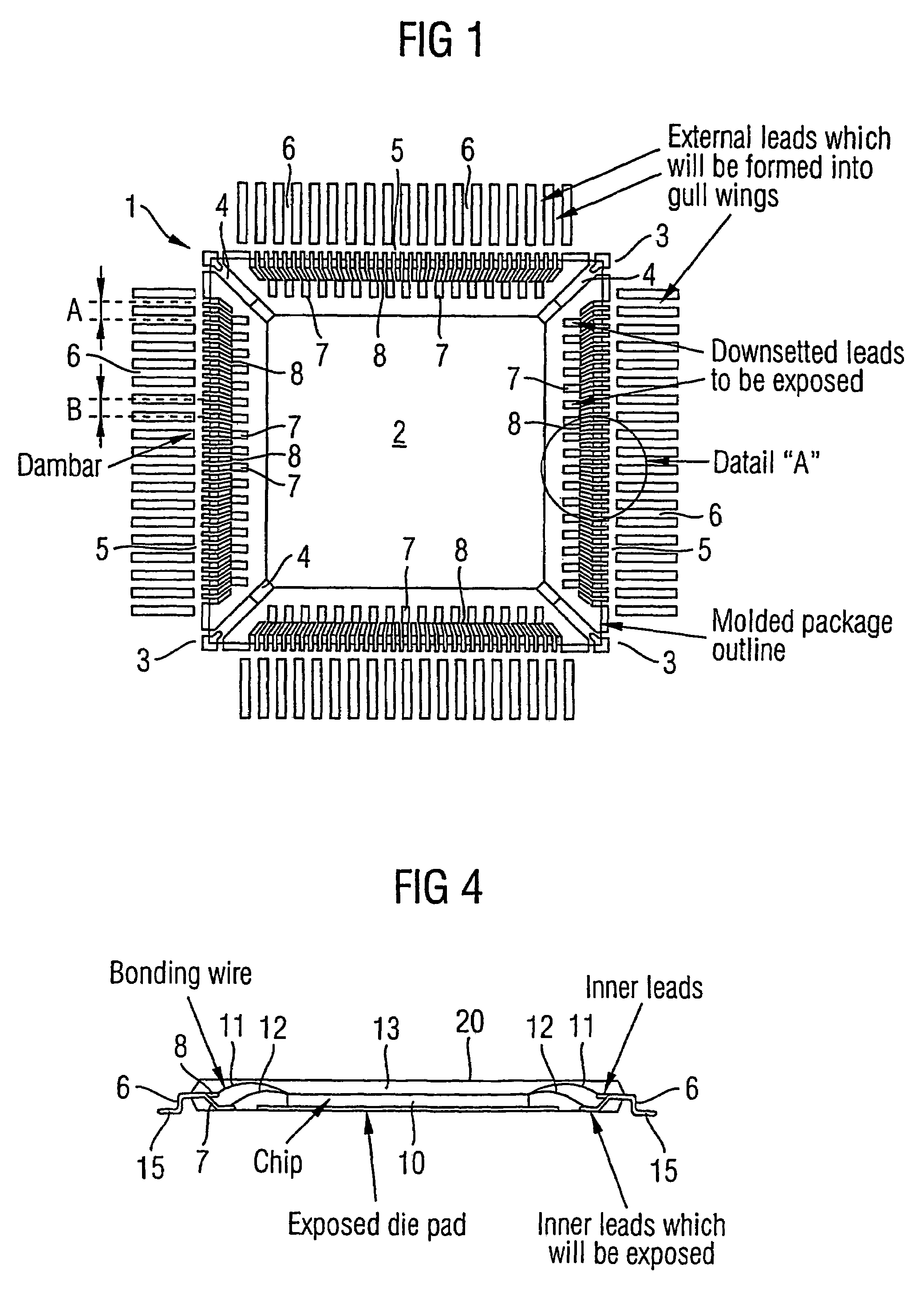
[0027]FIG. 1 shows a part of a lead frame 1, which includes a die pad 2 and a contact pin portion 3, which surrounds the die pad 2. The die pad 2 is connected to the contact pin portion 3 by supports 4.

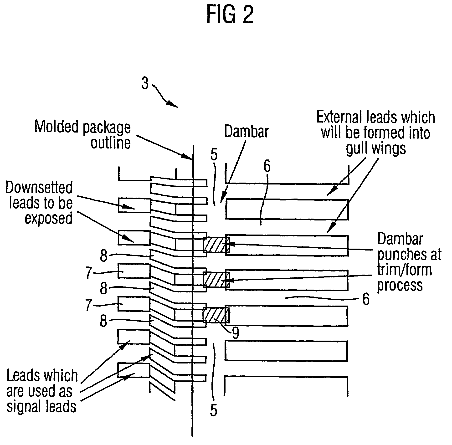
[0028]The contact pin portion 3 comprises a central section 5 commonly known as a dambar, which extends substantially parallel to each of the sides of the die pad 2. The dambar 5 has a set of first electrical contacts 6 extending from the dambar 5 in a direction away from the die pad 2. In addition, there are a set of second electrical contacts 7 extending from the dambar 5 in a direction towards the die pad 2. Located between each pair of adjacent second electrical contacts 7 is a bond member 8. The arrangement of the first and second contact members and the bond members 8 on the dambar 5 is shown in more detail in FIG. 2. The bond members 8 are arranged to be in-line with the first electrical contacts 6, and the second electrical contacts 7 are offset from the first electrical conta...


PUM


Abstract

A lead frame (1) has a first portion (2) adapted to have a semiconductor device (10) mounted thereon and a second portion (3) including a main member (5), a number of first contact members (6) and a number of second contact members (7). The first and second contact members (6, 7) depend from the main member (5). The second portion (3) at least partially surrounds the first portion (6). The first contact members (6) extend form the main member (5) in a direction away for the first portion (2) and the second contact members (7) extend from the main member (5) in a direction towards the first portion (2).

Description

[0001]This application is a continuation of co-pending International Application No. PCT / SG02 / 00014, filed Feb. 1, 2002, which designated the United States and was published in English.TECHNICAL FIELD[0002]The invention relates to a lead frame, and especially a lead frame for mounting a semiconductor device thereon.BACKGROUND[0003]Due to higher system integration, there is a trend to increase the number of input / output pins (i.e., pin count) on integrated circuit packages. At the same time, there is also a desire to reduce the package size. However, the increase in pin count places a limitation on the reduction of the package size, unless the pitch of the pins is reduced. Reducing the pitch of the pins leads to more complication during fabrication as it requires processes, such as stamping tool fabrication, dambar cut process, testing and surface mount technology to be more accurate.[0004]Therefore, there is a conflict between increasing system integration, which results in a higher...

Claims


Application Information

Patent Timeline
Patent Type & Authority Patents(United States)
IPC IPC(8): H01L23/495H01L23/28H01L23/48H01L23/52
CPCH01L23/49541H01L23/49551H01L2224/48091H01L24/48H01L2224/49109H01L2224/48247H01L24/49H01L23/4334H01L2924/00014H01L2924/00H01L2224/05599H01L2224/45099H01L2224/85399H01L2924/14H01L2924/181H01L2924/00012H01L2224/45015H01L2924/207
Inventor HONG, HENG WANYIP, TIAN SIANGTAN, JOO HONGLEE, CHOON MUAHKOH, LIANG KNG IAN
Owner INFINEON TECH AG
Why Eureka
Try Eureka