Memory array with current limiting device for preventing particle induced latch-up

Active Publication Date: 2007-03-27
INFINEON TECH LLC
View PDF12 Cites 10 Cited by
  • Summary
  • Abstract
  • Description
  • Claims
  • Application Information

AI Technical Summary

Benefits of technology

[0046]According to one aspect of the embodiments, each column has a latch-up holding current value. In addition, each impedance element can limit the current supplied to

Problems solved by technology

As integrated circuit devices continue to shrink in size errors and failures due to sub-atomic particles have become more problematic.
Particle induced errors and failures are most often attributed to alpha particles traveling through a semiconductor substrate and generating electron hole pairs.
At larger geometry sizes (i.e., larger well sizes), the number of electron hole pairs generated by a particle may not be sufficient to induce error or failure.
However, in smaller geometry structures, such as memory arrays, the number of generated electron hole pairs can be significant with respect to the relatively small size of wells and devices.
However, for complementary metal-oxide-semiconductor (CMOS) type circu

Method used


Image

  • Memory array with current limiting device for preventing particle induced latch-up
  • Memory array with current limiting device for preventing particle induced latch-up
  • Memory array with current limiting device for preventing particle induced latch-up

Examples


Example

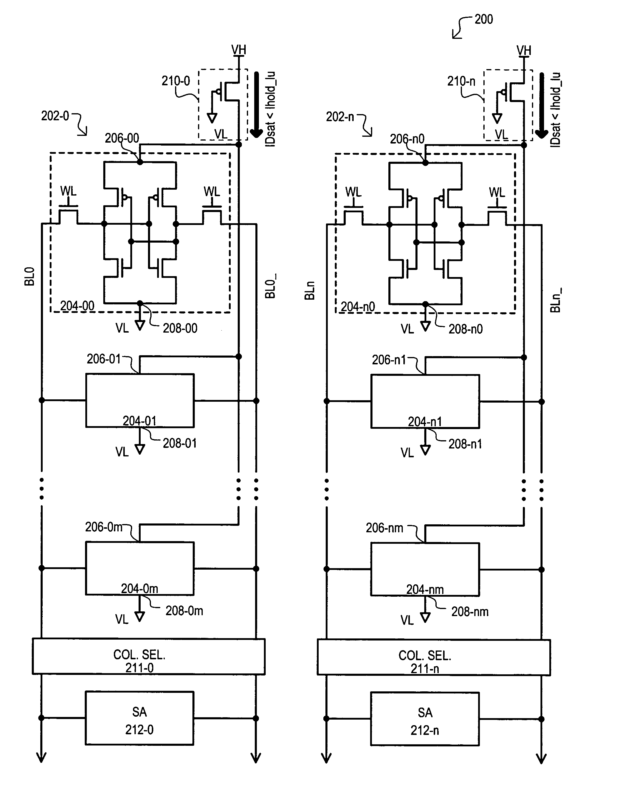
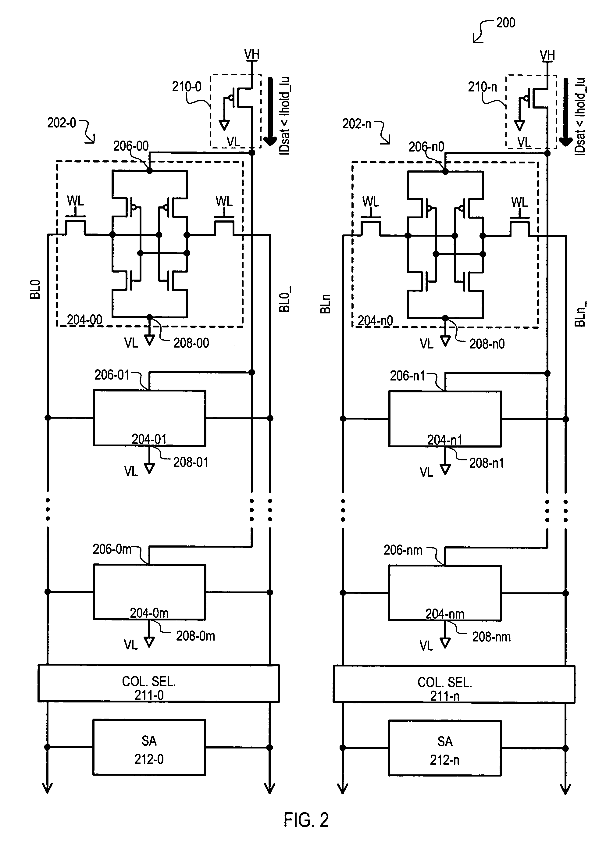
[0065]Referring now to FIG. 2, a memory cell array according to a second embodiment is set forth a block schematic diagram and designated by the general reference character 200. A memory cell array 200 can include a number of columns (202-0 to 202-n) that can each include a number of memory cells (204-00 to 204-nm). Each memory cell (204-00 to 204-nm) can receive power by way of a first cell supply node (206-00 to 206-nm) and second cell supply node (208-00 to 208-nm).

[0066]In the very particular example of FIG. 2, each memory cell (204-00 to 204-nm) can be connected to a corresponding complementary bit line pair (BL0 / BL0_ to BLn / BLn_). Thus, those memory cells (204-00 to 204-0m) commonly coupled to bit line pair (BL0 / BL0_) can form a memory cell column 202-0, and memory cells (204-n0 to 204-nm) commonly coupled to bit line pair (BLn / BLn_) can form a memory cell column 202-n.

[0067]In addition, each memory cell (204-00 to 204-nm) in the example of FIG. 2 is a six transistor (6-T) me...

Example

[0074]Referring now to FIG. 3, a memory cell array according to a third embodiment is set forth a block schematic diagram and designated by the general reference character 300. A memory cell array 300 can have some of the same general structures as that shown in FIG. 2. Accordingly, like sections will be referred to by the same reference character but with the first digit being a “3” instead of a “2”.

[0075]A third embodiment 300 can differ from that of FIG. 2 in that current limiting devices (310-0 to 310-n) can be resistors instead of transistors. In such an arrangement, resistors of the current limiting devices (310-0 to 310-n) can also limit current drawn in a particle event to less than a latch-up holding current. One skilled in the art could arrive at the appropriate resistance needed to limit current by a desired amount according to power supply levels VH, VL and corresponding memory cell characteristics.

[0076]In this way, a resistor can provide current limiting on a column-by...


PUM


Abstract

A memory device can include a group of memory cells, which can be arranged in a column (100) that receives power by way of a first cell supply nodes (106-0 to 106-m). A current limiter (110) can be situated between first cell supply nodes (106-0 to 106-m) and a power supply (VH), and limit a current (llimit) to less than a latch-up holding current (lhold_lu) for the group of memory cells (100). In a particle event, such as an α-particle strike, a current limiter (110) can prevent a latch-up holding current (lhold_lu) from developing, thus preventing latch-up from occurring. Current limiter (110) can include p-channel transistors and/or resistors, and thus consume a relatively small area of the memory device.

Description

TECHNICAL FIELD[0001]The present invention relates generally to devices having memory arrays, and more particularly to memory arrays with structures for reducing particle induced latch-up.BACKGROUND OF THE INVENTION[0002]As integrated circuit devices continue to shrink in size errors and failures due to sub-atomic particles have become more problematic. Particle induced errors and failures are most often attributed to alpha particles traveling through a semiconductor substrate and generating electron hole pairs. Such alpha particles may be generated by the decay of elements (e.g., uranium, thorium) or cosmic ray events, as but a few examples.[0003]At larger geometry sizes (i.e., larger well sizes), the number of electron hole pairs generated by a particle may not be sufficient to induce error or failure. However, in smaller geometry structures, such as memory arrays, the number of generated electron hole pairs can be significant with respect to the relatively small size of wells and...

Claims


Application Information

Patent Timeline
IPC IPC(8): G11C11/00
CPCG11C11/413
Inventor TZOU, JOSEPHMAJJIGA, JITHENDERWHATELY, MORGANTRAN, THINH
Owner INFINEON TECH LLC
Why Eureka
Try Eureka