Plating-rinse-plating process for fabricating copper interconnects

a copper interconnect and plating technology, applied in the field of plating-rinse-plating process for fabricating copper interconnects, can solve the problems of increasing the difficulty of a cmp process, requiring longer overpolish time for copper protrusion, and not being applicable to the sputtering process widely used for al metallization, so as to achieve better sheet resistance control and easy cmp.

Inactive Publication Date: 2007-04-03
TEXAS INSTR INC
View PDF11 Cites 2 Cited by
  • Summary
  • Abstract
  • Description
  • Claims
  • Application Information

AI Technical Summary

Benefits of technology

[0006]An advantage of the invention is providing an ECD process that provides a smooth film that is easier to CMP and provides better sheet resistance control.
[0007]This and other advantages will be apparent to those of ordinary skill in the art having reference to the specification in conjunction with the drawings.

Problems solved by technology

The sputtering process widely used for Al metallization is not applicable to Cu metallization due to its inherent limitation in step coverage.
Chemical vapor deposition (CVD) used in tungsten (W) metallization is not preferred for Cu at this time due to issues with morphology, adhesion and the conformal nature (seam formation issue) of CVD Cu films.
The copper protrusion requires longer overpolish time and otherwise increases the difficultly of a CMP process.
As device features continue to shrink and density continues to increase, the protrusion problem becomes more and more significant.

Method used


Image

  • Plating-rinse-plating process for fabricating copper interconnects
  • Plating-rinse-plating process for fabricating copper interconnects
  • Plating-rinse-plating process for fabricating copper interconnects

Examples


Embodiment Construction

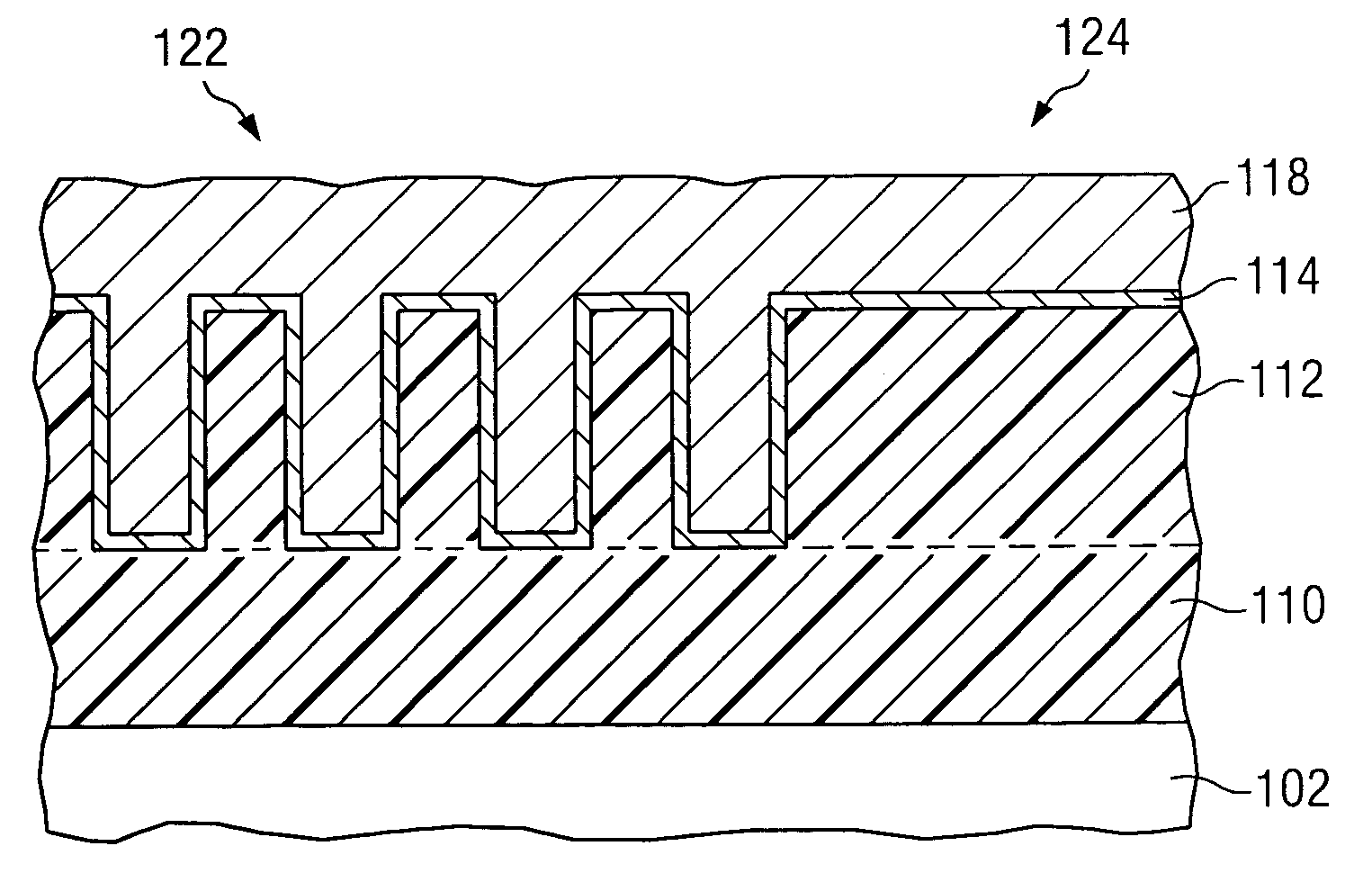
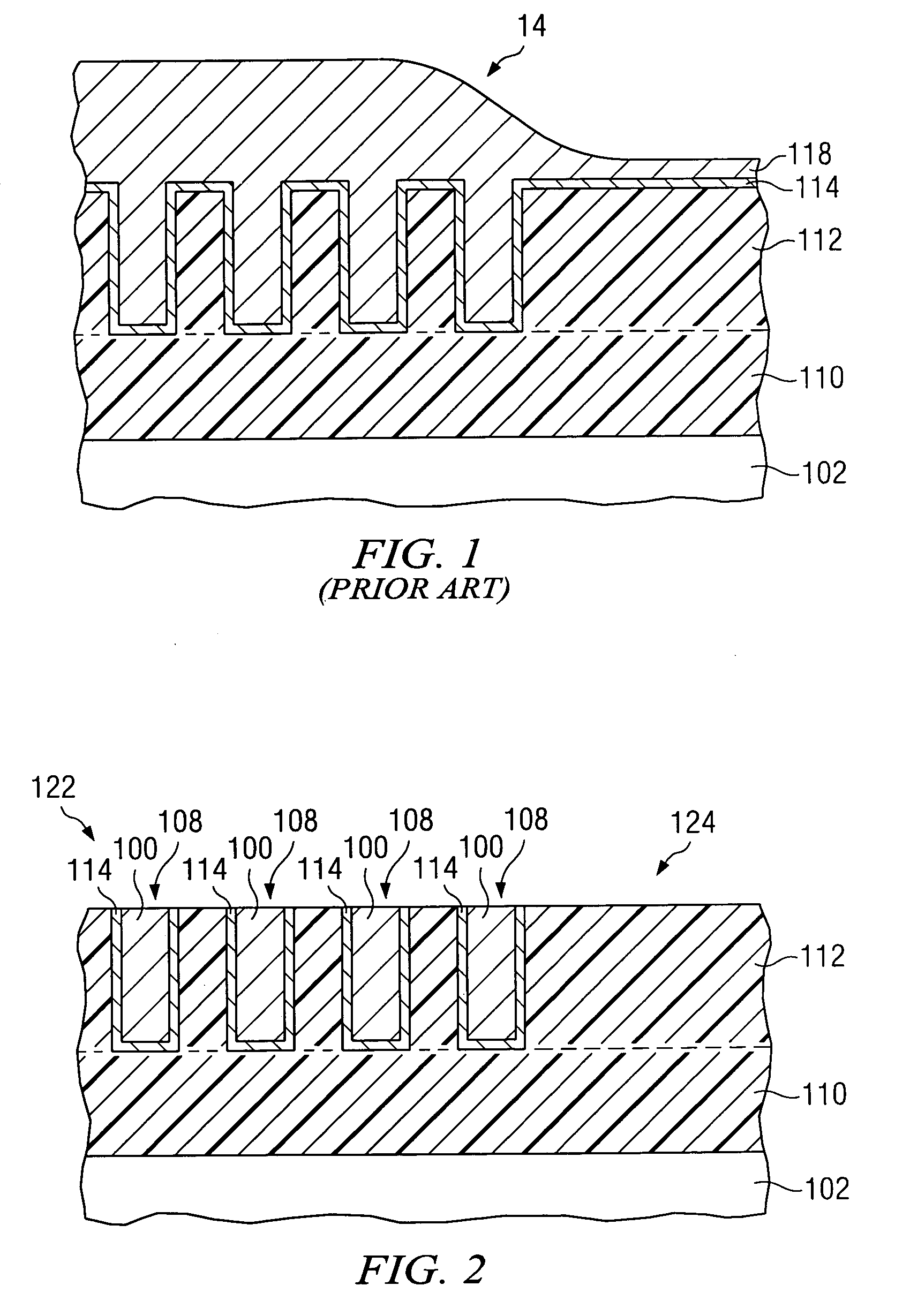
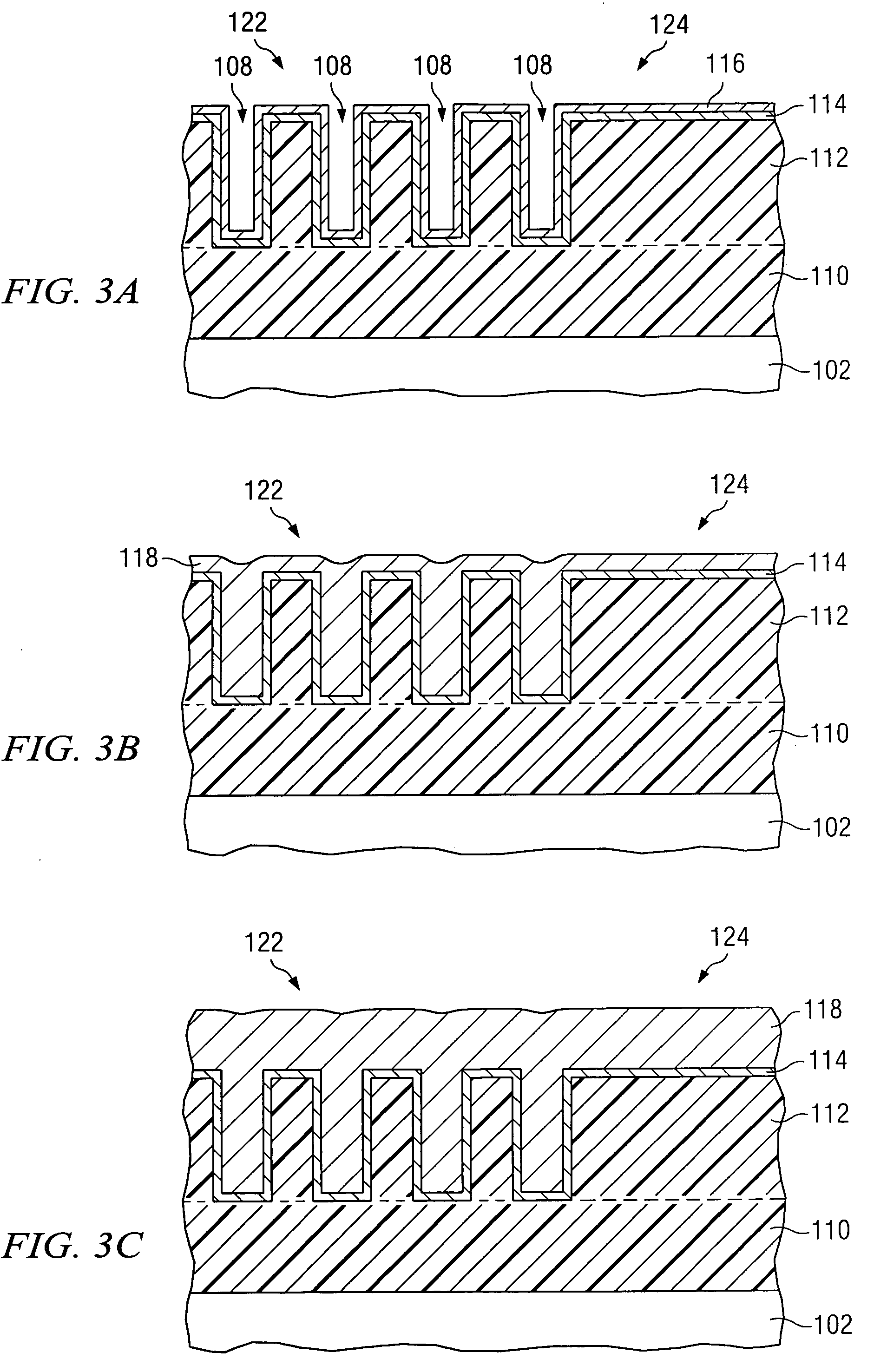
[0012]The invention will now be described in conjunction with dual damascene copper interconnect process. It will be apparent to those of ordinary skill in the art having reference to the specification that the benefits of the invention may be applied to ECD copper in general where it is desired to fill dense features.

[0013]A dual damascene copper interconnect 100 formed according to the invention is shown in FIG. 2. Copper interconnect 100 is formed over semiconductor body 102. Semiconductor body 102 typically has transistors and other devices (not shown) formed therein. Semiconductor body 102 may also include one or more additional metal interconnect layers (not shown). Copper interconnect 100 comprises a lead portion formed within trenches 108. A via portion (not shown) may also be formed below trenches 108. Vias extend from the bottom of trenches 108 through interlevel dielectric (ILD) 110 to a lower metal interconnect layer. Trenches 108 are formed within intrametal dielectric ...


PUM

PropertyMeasurementUnit
temperatureaaaaaaaaaa
pHaaaaaaaaaa
temperatureaaaaaaaaaa

Abstract

An improved copper ECD process. After the copper seed layer (116) is formed, a first portion of copper film (118) is plated onto the surface of the seed layer (116). The surface of the first portion of the copper film (118) is then rinsed to equalize the organic adsorption on all sites to prevent preferential copper growth in dense areas. After rinsing, the remaining copper of the copper film (118) is electrochemically deposited.

Description

FIELD OF THE INVENTION[0001]The invention is generally related to the field of forming copper interconnects in semiconductor devices and more specifically to electrochemical deposition of copper interconnects.BACKGROUND OF THE INVENTION[0002]Copper (Cu) metallization is gaining momentum in replacing aluminum (Al), particularly for the 0.18 um technology node and beyond. Due to the difficulty in dry etching Cu, a damascene approach is widely used for Cu metallization. This requires the Cu metallization process to have a high gap fill capability. The sputtering process widely used for Al metallization is not applicable to Cu metallization due to its inherent limitation in step coverage. Chemical vapor deposition (CVD) used in tungsten (W) metallization is not preferred for Cu at this time due to issues with morphology, adhesion and the conformal nature (seam formation issue) of CVD Cu films. Currently, the only manufacturable process for depositing Cu for interconnect applications is ...

Claims


Application Information

Patent Timeline
Patent Type & Authority Patents(United States)
IPC IPC(8): C25D5/48C25D5/02C25D5/10C25D7/12H01L21/288H01L21/3205H01L21/768H01L23/52
CPCH01L21/2885H01L21/76877
Inventor CHEN, LINLINLU, JIONG-PINGXIA, CHANGFENG
Owner TEXAS INSTR INC
Why Eureka
Try Eureka