Impedance qualization module

a technology of qualization module and qualization module, which is applied in the direction of electrical apparatus construction details, fixed capacitor details, coupling device connections, etc., can solve the problems of reducing bandwidth and more hardware, reducing performance, and affecting the operation of high-frequency digital circuits

Inactive Publication Date: 2007-04-03
THIN FILM TECH
View PDF3 Cites 33 Cited by
  • Summary
  • Abstract
  • Description
  • Claims
  • Application Information

AI Technical Summary

Benefits of technology

[0008]It is a primary object of the present invention to provide a passive thin film device that can be coupled to compensate for signal attenuation and / or degradation occurring in conductors conveying signals at gigahertz frequencies.

Problems solved by technology

Dielectric and conductor losses, cross talk, reflections and noise, among a variety of other parasitic and signal degrading conditions, can impair operation of high frequency digital circuits, such as used in many telecommunication and networking applications.
These problems are especially apparent at frequencies and data transfer rates in excess of 1.0 GHz, where reduced performance means reduced bandwidth and more hardware to achieve any desired result.
Cross talk can develop between signal lines and reflections and noise can develop from terminations.
The resultant losses or signal attenuation, noise and cross talk can distort and reduce the fidelity of transmitted data signals.
Delays can also occur with a resultant loss of synchronization in data conveyed between data supply conductors and responding circuitry.
The degradation of signal fidelity and loss of synchronization make it difficult to distinguish the information content of transmitted data.
High frequency circuit designers therefore expend considerable effort to minimize sources of noise, cross talk and signal attenuation.
Such devices, however, frequently require increased power and increased physical space for the circuitry.
These improvements can also be relatively costly to implement.
Such mountings can be costly to implement and cannot be readily re-worked, if changes or fine-tuning is required.

Method used


Image

  • Impedance qualization module
  • Impedance qualization module
  • Impedance qualization module

Examples


Embodiment Construction

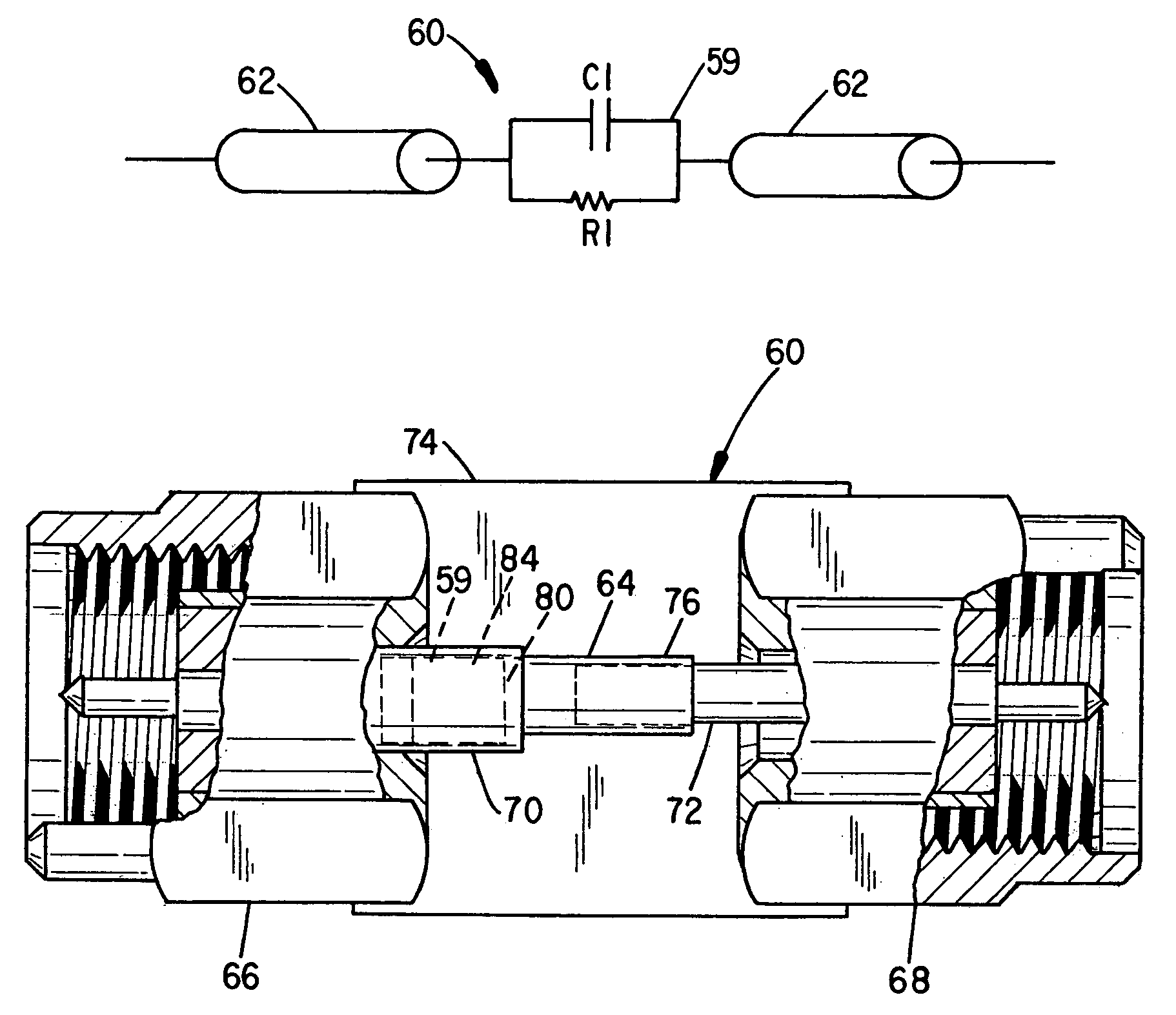
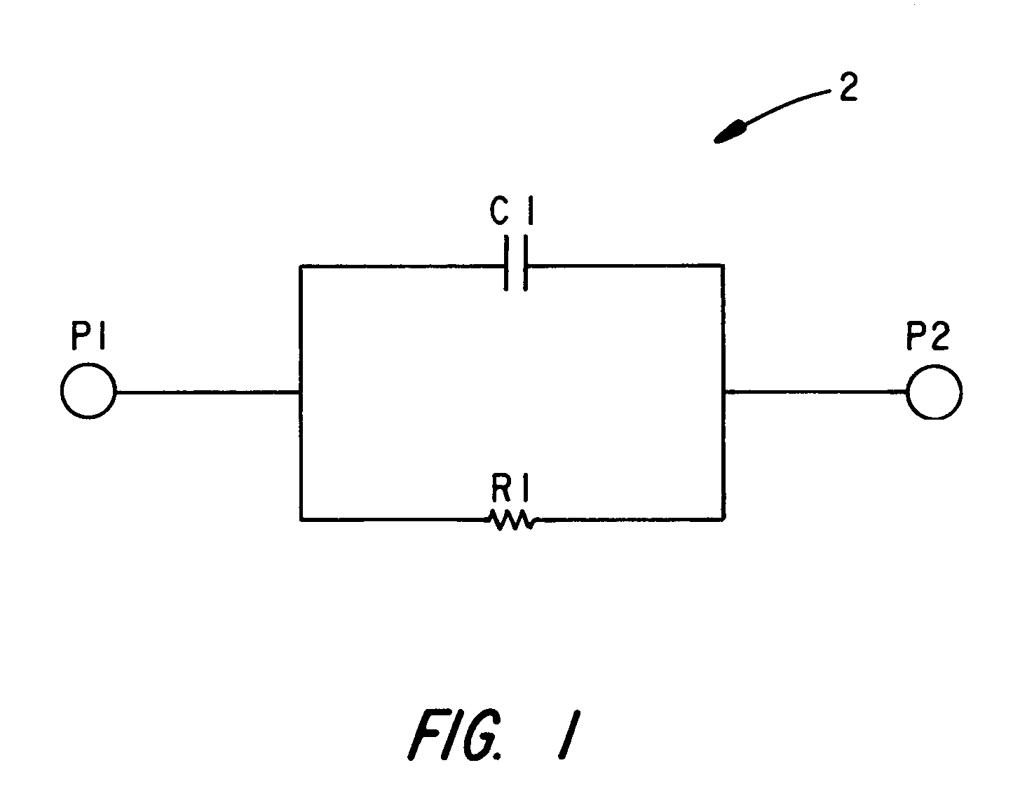
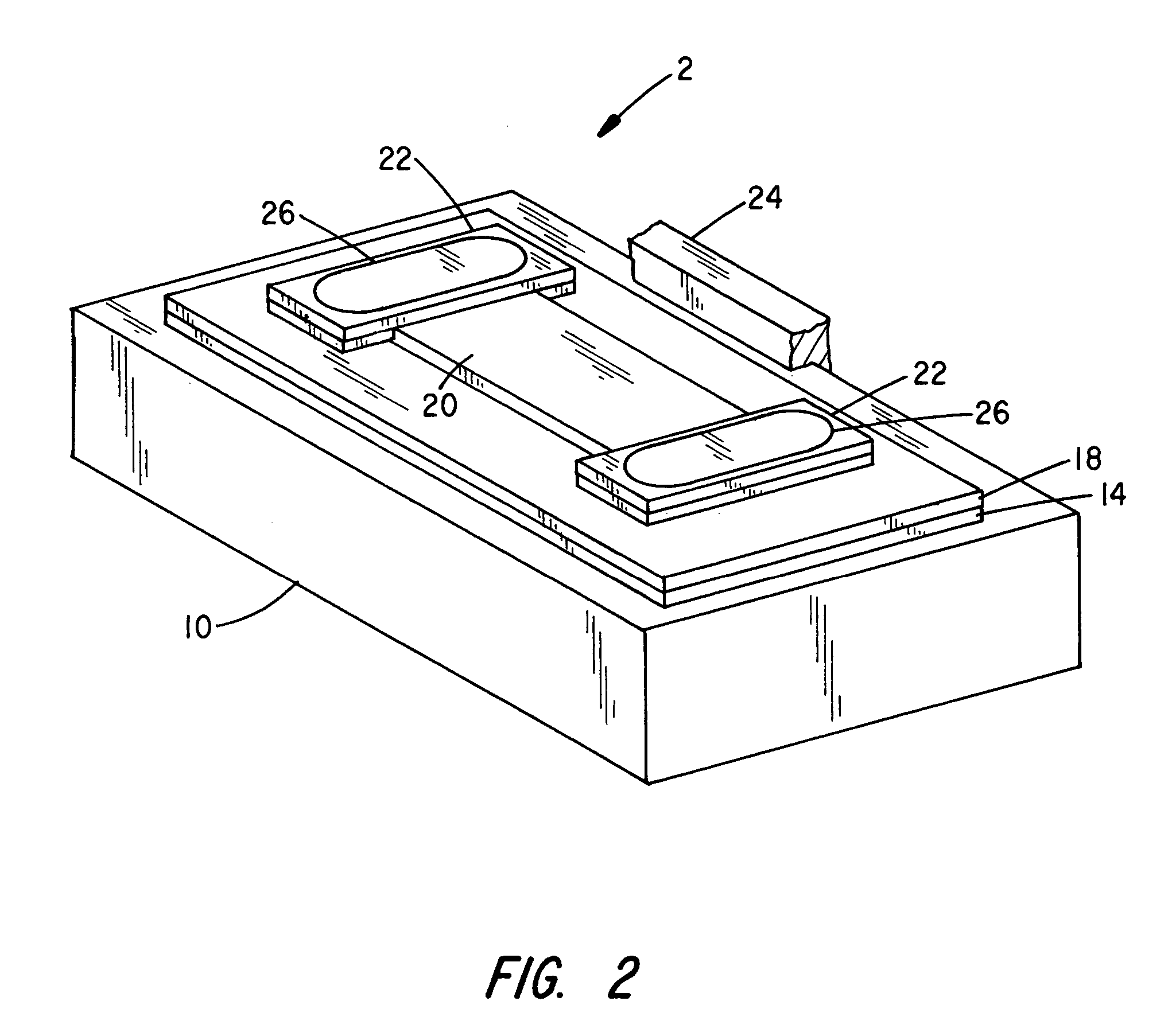
[0041]Referring to FIGS. 1–4, views are shown to a passive thin film equalizer device 2. The device 2 can be coupled to conductors conveying signals at frequencies in excess of 1.0 GHZ to reduce conductor losses and improve signal integrity. The device 2 is typically constructed to condition a specific length of conductor. Longer conductors can be conditioned with several displace, serially arranged devices.

[0042]With attention to FIG. 1, the device 2 includes a capacitor element C1 and resistor element R1 that are coupled in parallel relative to input and output ports P1 and P2. The device 2 is typically coupled in series with a conductive path that is being conditioned, for example a printed circuit trace conductor or transmission line. The ports P1 and P2 can be coupled at any convenient location along the conductive path, including printed circuit terminations, such as in associated connectors.

[0043]Depending upon the length of the lossy conductor, the values of R1 and C1 can be...


PUM


Abstract

A thin film circuit module constructed for serial coupling to circuit conductors at printed and transmission line circuits. In one form of equalizer construction, thin film circuit elements are deposited on a supporting substrate and wherein a capacitor plate is defined a circuit resistor. Two connector applications serially couple the equalizer modules to trace conductors of a motherboard connector block and to cylindrical core conductors of a coaxial connector. Other hybrid equalizer constructions provide modules constructed of thin film resistors and pick-and-placed capacitors mounted piggyback to an equalizer module substrate.

Description

[0001]This is a continuation-in-part of application Ser. No. 10 / 313,215 filed Dec. 6, 2002, now U.S. Pat. No. 6,819,569, issued Nov. 16, 2004.BACKGROUND OF THE INVENTION[0002]The present invention relates to passive thin film devices that compensate for signal losses over trace conductors at printed circuit assemblies and / or connectors and / or transmission lines and passively augment the impedance characteristic of the relevant conductive pathway, among other applications.[0003]Dielectric and conductor losses, cross talk, reflections and noise, among a variety of other parasitic and signal degrading conditions, can impair operation of high frequency digital circuits, such as used in many telecommunication and networking applications. These problems are especially apparent at frequencies and data transfer rates in excess of 1.0 GHz, where reduced performance means reduced bandwidth and more hardware to achieve any desired result.[0004]Cross talk can develop between signal lines and re...

Claims


Application Information

Patent Timeline
Patent Type & Authority Patents(United States)
IPC IPC(8): H05K7/02H05K7/06H05K7/08H05K7/10H01C13/00H01G4/228H01G4/40H01L27/01H01R13/6466H01R13/6474H01R13/719H01R24/38H03H1/00H03H7/01
CPCH01G4/40H01L27/016H01R13/719H01R24/44H01R23/6873H01R23/7073H01R2103/00H01R12/724H01R13/658
Inventor BROMAN, MARK HAMILTONHOWIESON, MIKETAKAMURA, TSUGUHIKOBROOKS, MARKOKAMOTO, YASUTSUGUHUIBREGTSE, BRENT
Owner THIN FILM TECH
Why Eureka
Try Eureka