Doped absorption for enhanced responsivity for high speed photodiodes

a photodiode and absorption technology, applied in the field of photodiodes, can solve the problems of reduced carrier mobility, low responsivity and hence low sensitivity, and severe compromis

Inactive Publication Date: 2007-04-10
LUMENTUM OPERATIONS LLC
View PDF27 Cites 42 Cited by
  • Summary
  • Abstract
  • Description
  • Claims
  • Application Information

AI Technical Summary

Problems solved by technology

The Ishibashi et al. disclosure teaches a pin diode with high-saturation power; this is at a cost of low responsivity and hence low sensitivity.
However, severe compromises must be made when the two devices integrated, in this instance, the p-i-n photodiode and the transistor, are very different and require opposite optimization schemes.
The heavy doping of the base also reduces carrier mobility, and therefore, reduces the base transit speed.
On the other hand, the very heavy doping in the thin base for example 1e19 cm−3, adversely affects the photodiode speed by reducing the carrier mobility, and adversely affects responsivity by enhancing minority carrier recombination.
As a result, the heavily doped thin base InGaAs layer minimally improves the responsivity-bandwidth-product (RBP), if at all.
In practice, it is not possible to produce a semiconductor to have absolutely zero dopant atom therein.

Method used


Image

  • Doped absorption for enhanced responsivity for high speed photodiodes
  • Doped absorption for enhanced responsivity for high speed photodiodes
  • Doped absorption for enhanced responsivity for high speed photodiodes

Examples


Embodiment Construction

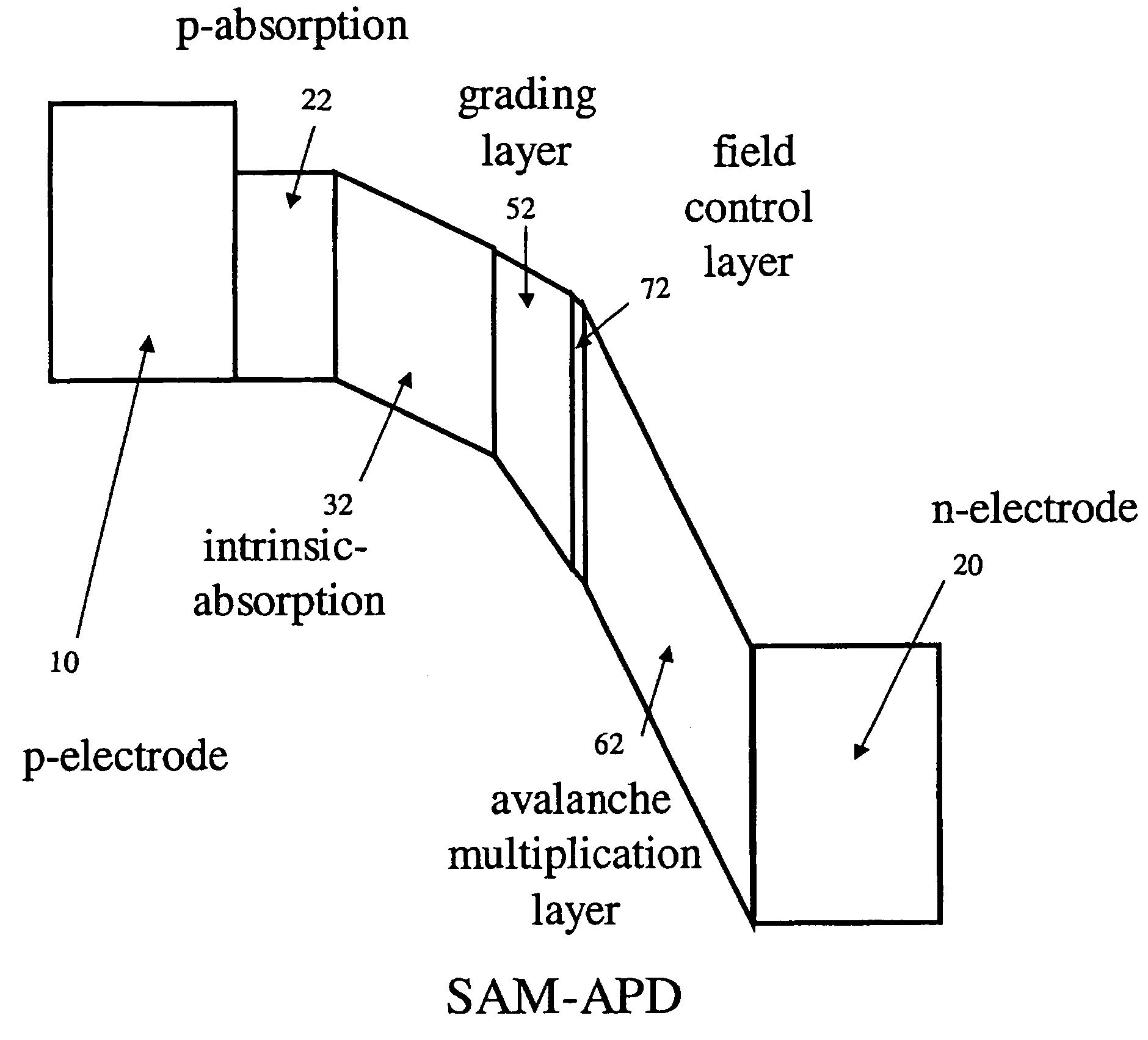
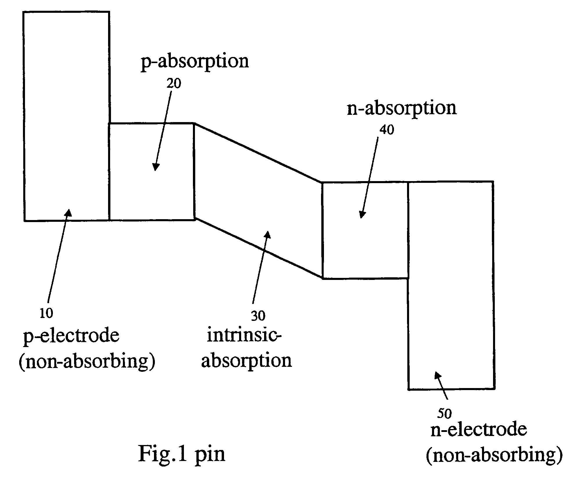
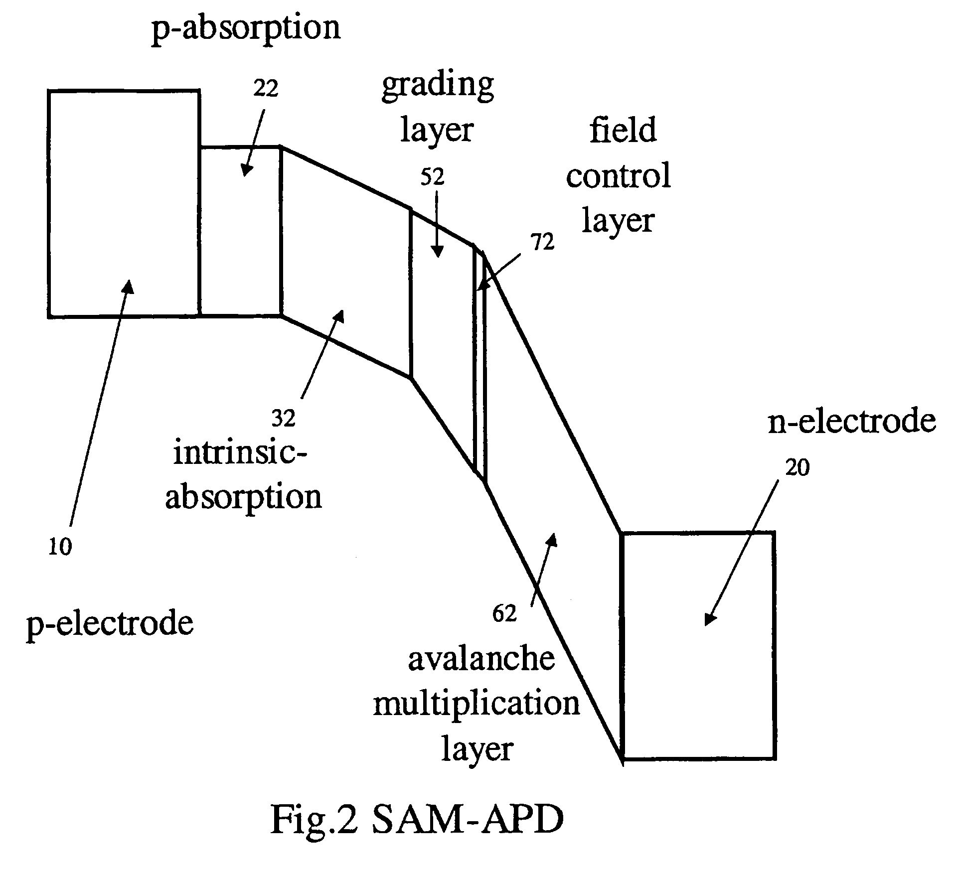
[0032]Unfortunately, in a conventional pin, there is a tradeoff between speed and responsivity. To achieve high-speed, a device requires thin absorption layers so that carriers can pass through quickly before they enter the electrode. On the other hand, to achieve high responsivity, a thick absorption layer is required so that most or all photon energy is absorbed and few or none of photons are lost. This is true when the incident light is normal to the epitaxial layers. As a result, for a conventional pin, the speed X responsivity or the responsivity-bandwidth product as it is known, is essentially a constant for surface-normal light incidence. The device described by Ishibashi described heretofore, is very poor with regard to its responsivity and sensitivity but higher saturation power is attained.

[0033]In accordance with this invention, surprisingly, the speed X responsivity limit can be increased; this is of paramount importance for a high-speed avalanche photodiodes (APDs); in ...


PUM


Abstract

A photodiode with a semiconductor intrinsic light absorption layer has at least one p-doped light absorption layer or an n-doped light absorption layer, and preferably both. The diode also has a cathode electrode and an anode electrode electrically coupled with the p-doped light absorption layer or the n-doped light absorption layer.

Description

CROSS-REFERENCE TO RELATED APPLICATIONS [0001]The present application is a continuation-in-part application of U.S. patent application Ser. No. 10 / 304,202, filed on Nov. 26, 2002, now abandoned and claims priority of U.S. Provisional Patent Application No. 60 / 333,616 filed on Nov. 27, 2001, entitled “Doped Absorption for Enhanced Responsivity-Bandwidth Limit and Doped Quarternary Stack for the Reduction of Carrier Trapping in High-Speed High Sensitivity Photodiodes”, assigned to the assignee of the present application, and the disclosures of which are incorporated herein.FIELD OF THE INVENTION [0002]This invention relates to photodiodes, such as p-i-n photodiodes (PINs) and avalanche photodiodes (APDs); and, more particularly to a diode structure that provides an enhanced responsivity, and, therefore, enhanced sensitivity, without compromising speed.BACKGROUND OF THE INVENTION[0003]Various photodiode structures are known and the goal in designing these structures depends upon which ...

Claims


Application Information

Patent Timeline
Patent Type & Authority Patents(United States)
IPC IPC(8): H01L21/00H01L31/00H01L27/148H01L31/105H01L31/107
CPCH01L31/03046H01L31/0352H01L31/105H01L31/107H01L31/1075Y02E10/544
Inventor YAO, JIE
Owner LUMENTUM OPERATIONS LLC
Why Eureka
Try Eureka