Camera module for compact electronic equipments

a technology of electronic equipment and camera module, applied in the field of semiconductor devices, can solve the problems of miniaturization of the module, large size of the semiconductor device itself, etc., and achieve the effect of miniaturization of the camera modul

Active Publication Date: 2007-04-10
SOCIONEXT INC
View PDF16 Cites 16 Cited by
  • Summary
  • Abstract
  • Description
  • Claims
  • Application Information

AI Technical Summary

Benefits of technology

[0022]A more specific object of the present invention is to provide a miniaturized semiconductor device having resin bumps which is formed by effectively using an area in the bottom (mounting side) of the semiconductor device.
[0025]According to above-mentioned invention, so-called resin bumps are formed on the mounting surface of the semiconductor device. The resin bumps constituted by the second protruding parts among the resin bumps are formed in the area where no bumps are formed in a conventional semiconductor device, that is, the area directly under the semiconductor element. Thereby, in the semiconductor device according to the present invention, the resin bumps can be formed all over the entire mounting surface. Therefore, if the semiconductor device according to the present invention has the same size, a number of resin bumps can be increased as compared to the conventional semiconductor device. If, in other words, the resin bumps of the same number as the conventional semiconductor device are formed, the size of the semiconductor device can be reduced, thereby achieving a miniaturized semiconductor device. Additionally, since the resin bumps are also provided in the element mounting area, the degree of freedom in arrangement of the pattern wiring is increased which results in efficient wiring.
[0029]According to the above-mentioned invention, a space for providing the wiring pattern can be attained since the resin bumps are also arranged directly under the semiconductor element. Thus, high-density wiring can be achieved, which results in miniaturization of a camera module.

Problems solved by technology

Thus, if the semiconductor element becomes large and a number of electrodes is increased, there is a problem in that the size of the semiconductor device itself becomes large.
However, it is a subject to miniaturize a module while using the resin bump since the module size becomes inevitably large when forming the resin bumps with the encapsulation resin.

Method used


Image

  • Camera module for compact electronic equipments
  • Camera module for compact electronic equipments
  • Camera module for compact electronic equipments

Examples


Embodiment Construction

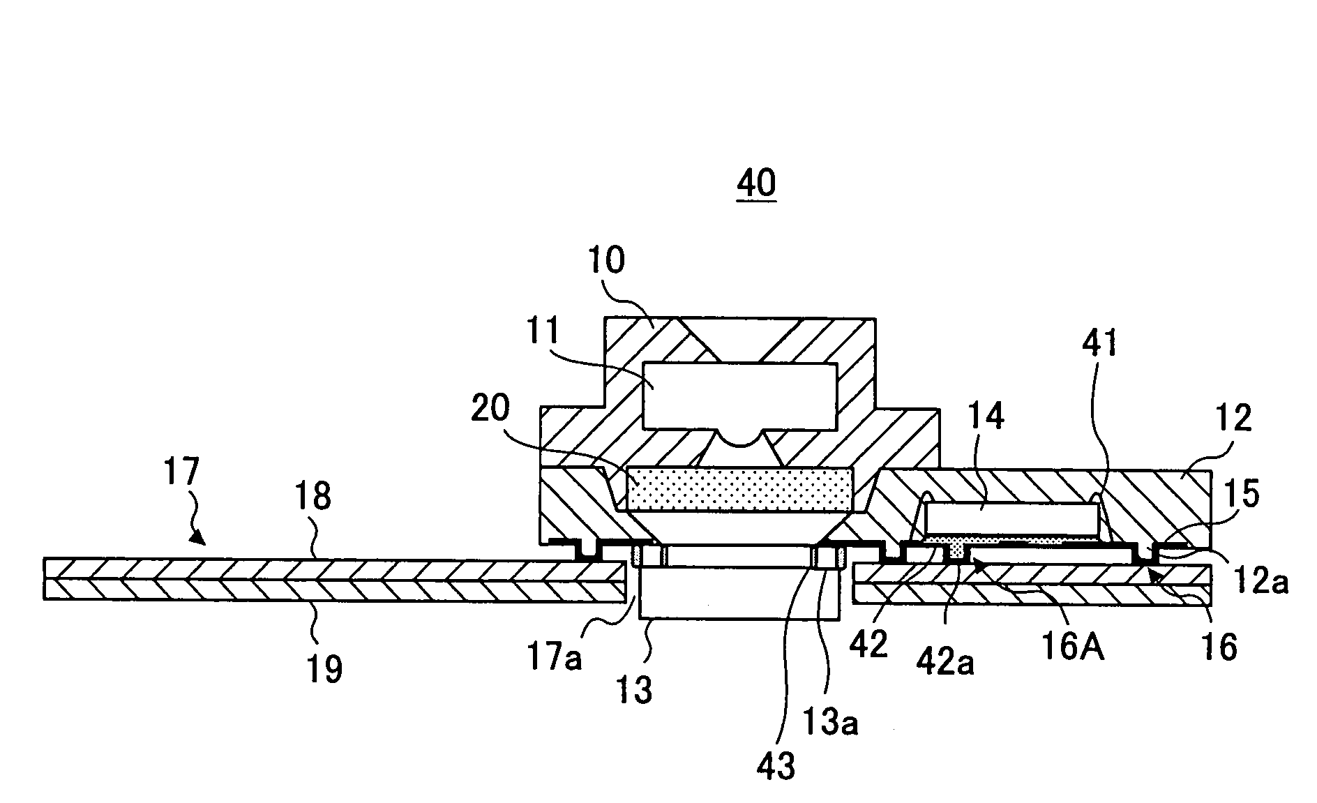
[0053]A description will now be given, with reference to FIG. 5, of a first embodiment of the present invention. FIG. 5 is a cross-sectional view of a semiconductor device 30 according to the first embodiment of the present invention. In FIG. 5, parts that are the same as the parts shown in FIG. 1 are given the same reference numerals.

[0054]The semiconductor device 30 according to the first embodiment of the present invention has a semiconductor element encapsulated by a mold resin 2 with a metal film 3 formed on a bottom surface (mounting surface) of the mold resin 2. The metal film 3 is patternized so as to form a wiring pattern. The semiconductor element 1 is arranged in the mold resin 2 in a face-up state where a circuit forming surface faces upward, and an element fixing resin 4 is provided on the backside of the semiconductor element 1. The element fixing resin 4 is an adhesive for fixing the semiconductor element 1 to a substrate in a manufacturing process thereof. Electrodes...


PUM


Abstract

In a camera module of a so-called multi-chip type, an imaging device and a semiconductor element for processing are mounted. The semiconductor element is encapsulated by a mold resin. Protruding parts are formed by the mold resin on a mounting surface of the mold resin. A metal film forming a pattern wiring is formed on the mounting surface of the mold resin. The metal film is also formed on the protruding parts so as to constitute external connection terminals together with the protruding parts. Electrodes of the semiconductor element are electrically connected to the pattern wiring. The protruding parts include first protruding parts positioned around the semiconductor element and second protruding parts formed in a mounting area of the semiconductor element on the mounting surface.

Description

BACKGROUND OF THE INVENTION[0001]1. Field of the Invention[0002]The present invention relates to semiconductor devices and, more particularly, to a semiconductor device suitable for a camera module which integrally packages a light-receiving element and an image-pickup lens.[0003]2. Description of the Related Art[0004]In recent years, portable telephones and portable personal computers equipped with a small camera have been developed. For example, a portable telephone equipped with a small camera picks up an image of a calling person by the small camera so as to acquire image data and sends the image data to a person on the line. Generally, such a small camera is constituted by a CMOS sensor and a lens.[0005]Miniaturization of portable telephones and portable personal computers has been progressed further, and there is also a demand for miniaturization of small cameras used for these equipments. In order to satisfy the demand for miniaturization of such a small camera, a camera modu...

Claims


Application Information

Patent Timeline
Patent Type & Authority Patents(United States)
IPC IPC(8): H01L27/00H01L21/48H01L21/56H01L21/68H01L23/00H01L23/12H01L23/31H01L25/10H01L25/18H01L27/146H01L27/148H01L31/0203H04N5/335
CPCH01L21/4832H01L21/563H01L21/568H01L23/3107H01L27/146H01L27/14618H01L27/14625H01L31/0203H01L2224/73203H01L2924/19041H01L2224/73204H01L2224/73265H01L2924/1815H01L2224/32225H01L2224/48227H01L2224/48091H01L24/73H01L2924/181H01L2224/83192H01L2924/18165H04N23/57H01L2924/00012H01L2924/00014H01L27/148H01L23/00
Inventor ONODERA, MASANORIMORIYA, SUSUMUKOBAYASHI, IZUMIAOKI, HIROSHIHONDA, TOSHIYUKI
Owner SOCIONEXT INC
Why Eureka
Try Eureka