Semiconductor device with withstand voltage structure and manufacturing method thereof

A voltage-resistant structure and semiconductor technology, applied in the fields of semiconductor devices, semiconductor/solid-state device manufacturing, electrical components, etc., can solve problems such as poor voltage-resistant performance, reduce production costs, ensure voltage-resistant performance, and reduce on-resistance. Effect

Active Publication Date: 2021-08-24
天津中科先进技术产业有限公司
View PDF3 Cites 0 Cited by
  • Summary
  • Abstract
  • Description
  • Claims
  • Application Information

AI Technical Summary

Problems solved by technology

[0003] In view of this, the object of the present invention is to provide a semiconductor device with a voltage-resistant structure and a manufacturing method thereof, so as to alleviate the technical problem of poor voltage-resistant performance of the device structure in the prior art

Method used


Image

  • Semiconductor device with withstand voltage structure and manufacturing method thereof
  • Semiconductor device with withstand voltage structure and manufacturing method thereof
  • Semiconductor device with withstand voltage structure and manufacturing method thereof

Examples


Embodiment 1

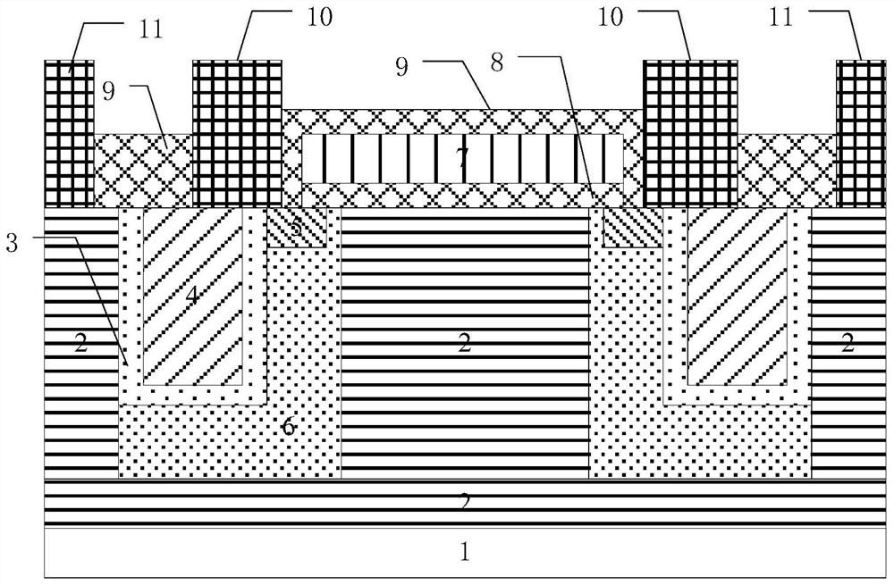
[0038] see figure 1, a cross-sectional view of a semiconductor device with a withstand voltage structure provided by an embodiment of the present invention. A semiconductor device with a voltage-resistant structure provided by an embodiment of the present invention includes: an N-type substrate 1, an N+ region 2, a P- body region 6, a voltage-resistant oxide layer 3, a polysilicon region 4, an N+ source region 5, a gate Extreme oxide layer 8, polysilicon gate 7, dielectric layer isolation 9, device source metal 10 and device drain metal 11. Wherein, the withstand voltage oxide layer and the polysilicon region constitute the withstand voltage structure of the semiconductor device. The N+ region is an electron drift region composed of a central region, a bottom region and a side region. The cross-section of the side area is "mouth", the cross-section of the central area is "one", located in the center of the side area, and the bottom area is square, located at the bottom of th...

Embodiment 2

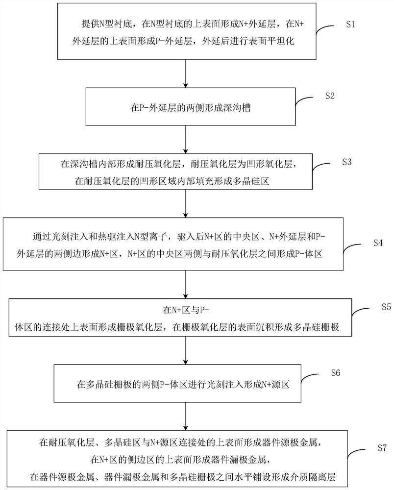
[0048] A method for manufacturing a semiconductor device with a withstand voltage structure provided by an embodiment of the present invention includes the following steps:

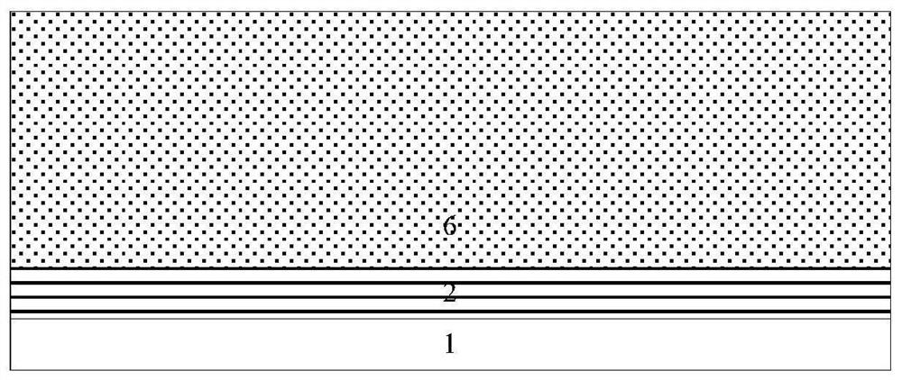
[0049] Step S1: providing an N-type substrate, forming an N+ epitaxial layer on the upper surface of the N-type substrate, forming a P- epitaxial layer on the upper surface of the N+ epitaxial layer, and performing surface planarization after epitaxy. see image 3 , a product schematic diagram of step S1 in the method for manufacturing a semiconductor device with a voltage-resistant structure provided in an embodiment of the present invention.

[0050] Step S2: forming deep trenches on both sides of the P- epitaxial layer. see Figure 4 , a product schematic diagram of step S2 in the method for manufacturing a semiconductor device with a voltage-resistant structure provided in an embodiment of the present invention.

[0051] Step S3: forming a voltage-resistant oxide layer inside the deep trench, the v...


PUM

PropertyMeasurementUnit
thicknessaaaaaaaaaa
widthaaaaaaaaaa
depthaaaaaaaaaa

Abstract

The invention provides a semiconductor device with a voltage-resistant structure and a manufacturing method thereof, relating to the technical field of semiconductor chips, including: an N-type substrate, an N+ region, a P-body region, a voltage-resistant oxide layer, a polysilicon region, and an N+ source region , gate oxide layer, polysilicon gate, dielectric layer isolation, device source metal and device drain metal. Wherein, the voltage-resistant oxide layer is respectively arranged on both sides of the central region of the N+ region, and is attached to the side regions of the N+ region respectively. within the shape area. This technical solution alleviates the technical problem of poor withstand voltage performance of the device structure in the prior art, effectively ensures the withstand voltage performance of the device, improves the saturation current of the semiconductor device, reduces the on-resistance of the device, and effectively utilizes the device area , reduces the production cost of the device, and improves the conduction performance of the semiconductor device.

Description

technical field [0001] The invention relates to the technical field of semiconductor chips, in particular to a semiconductor device with a withstand voltage structure and a manufacturing method thereof. Background technique [0002] At present, the structure of MOS devices mainly includes source metal, dielectric layer isolation, polycrystalline gate, gate oxide layer, device P-type body region, device N+ source region, device N-type epitaxial layer, device N-type substrate and Device drain metal. In the process of realizing the present invention, the inventors found that there are at least the following problems in the prior art: the on-resistance of the MOS device is large, and when the device is turned on, electrons will start from the N-type source, pass through the channel, and the N-type epitaxial layer. N-type substrate, eventually reaching the drain. To increase the withstand voltage of the device, the N-type epitaxial layer must be very thick, and the thicker the ...

Claims


Application Information

Patent Timeline
Patent Type & Authority Patents(China)
IPC IPC(8): H01L29/78H01L29/06H01L21/336
CPCH01L29/0684H01L29/66477H01L29/78
Inventor 王振海
Owner 天津中科先进技术产业有限公司
Why Eureka
Try Eureka