Integrated circuit

a technology of integrated circuits and circuits, applied in the direction of electronic switching, transistors, electrical equipment, etc., can solve the problems of occupying a large area on the substrate, and achieve the effect of increasing the route length and thus the effective resistance of the substra

Inactive Publication Date: 2007-04-10
MICRONAS
View PDF3 Cites 8 Cited by
  • Summary
  • Abstract
  • Description
  • Claims
  • Application Information

AI Technical Summary

Benefits of technology

[0014]To avoid the undesirable interaction between the transistors of the coupling circuit and the circuit components, at least one transistor of the coupling circuit may be surrounded by a shielding doping zone of the second conductivity type. A shielding doping zone of this type is biased in the nonconducting direction, such that a barrier layer is formed between this zone and the substrate.
[0015]The shielding doping zone preferably runs in an annular pattern along the surface of the substrate. The doping zone does not prevent every current flow from the at least one transistor of the coupling circuit through the substrate to the circuit component, but rather forces the charge carrier to follow an alternate route into the depth of the substrate. This increases the route length, and thus the effective resistance of the substrate, between the transistors of the coupling circuit and the circuit components. The contact doping zones of the coupling circuit are preferably surrounded by the shielding doping zone.

Problems solved by technology

The desirable isolation of the supply voltage systems for the individual circuit components may lead to problems in the event of excessive voltages, for example, electrical overstress (EOS).
Another problem with these conventional coupling circuits 3, 4 is the considerable area they utilize on the substrate.

Method used


Image

  • Integrated circuit
  • Integrated circuit
  • Integrated circuit

Examples


Embodiment Construction

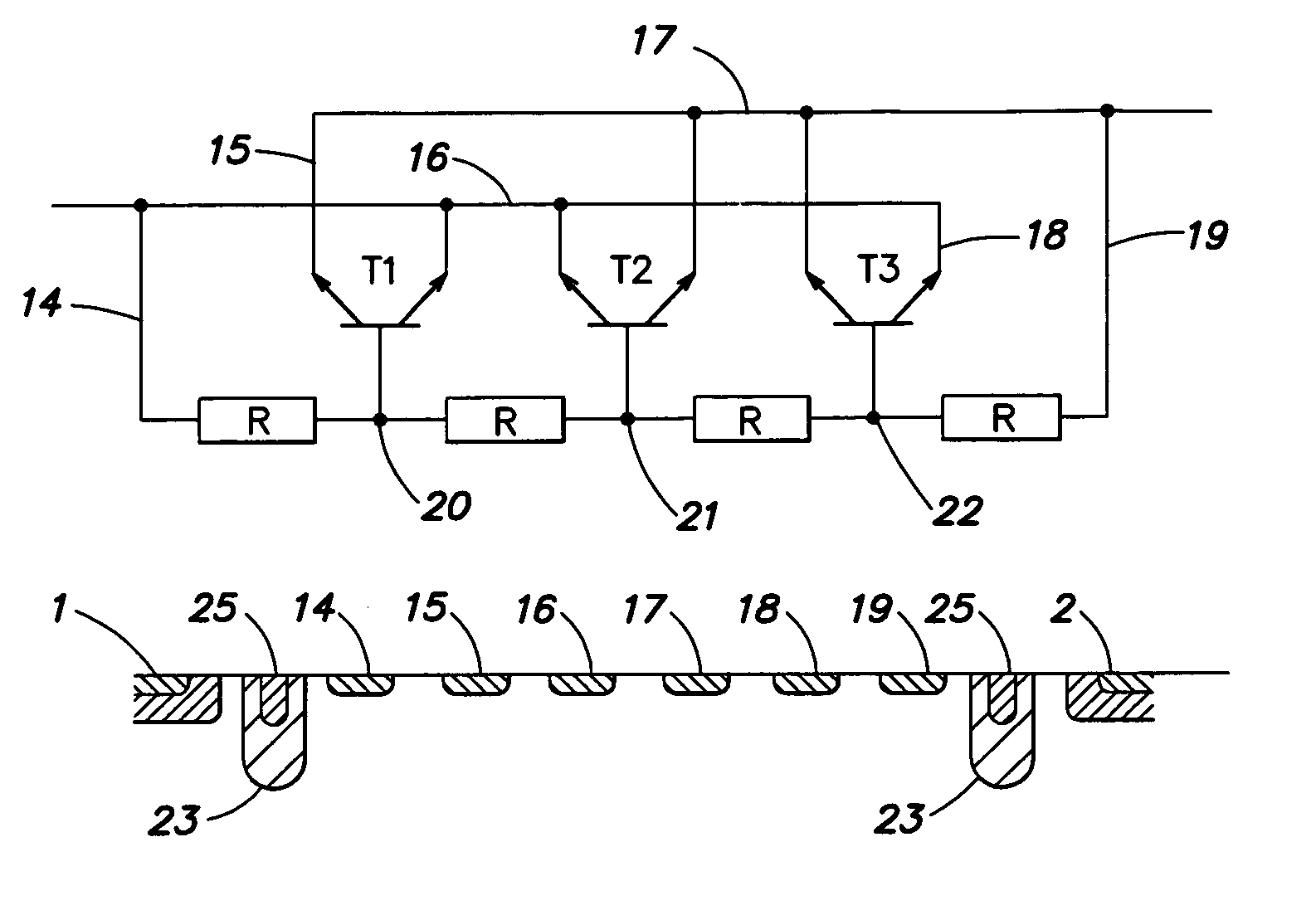
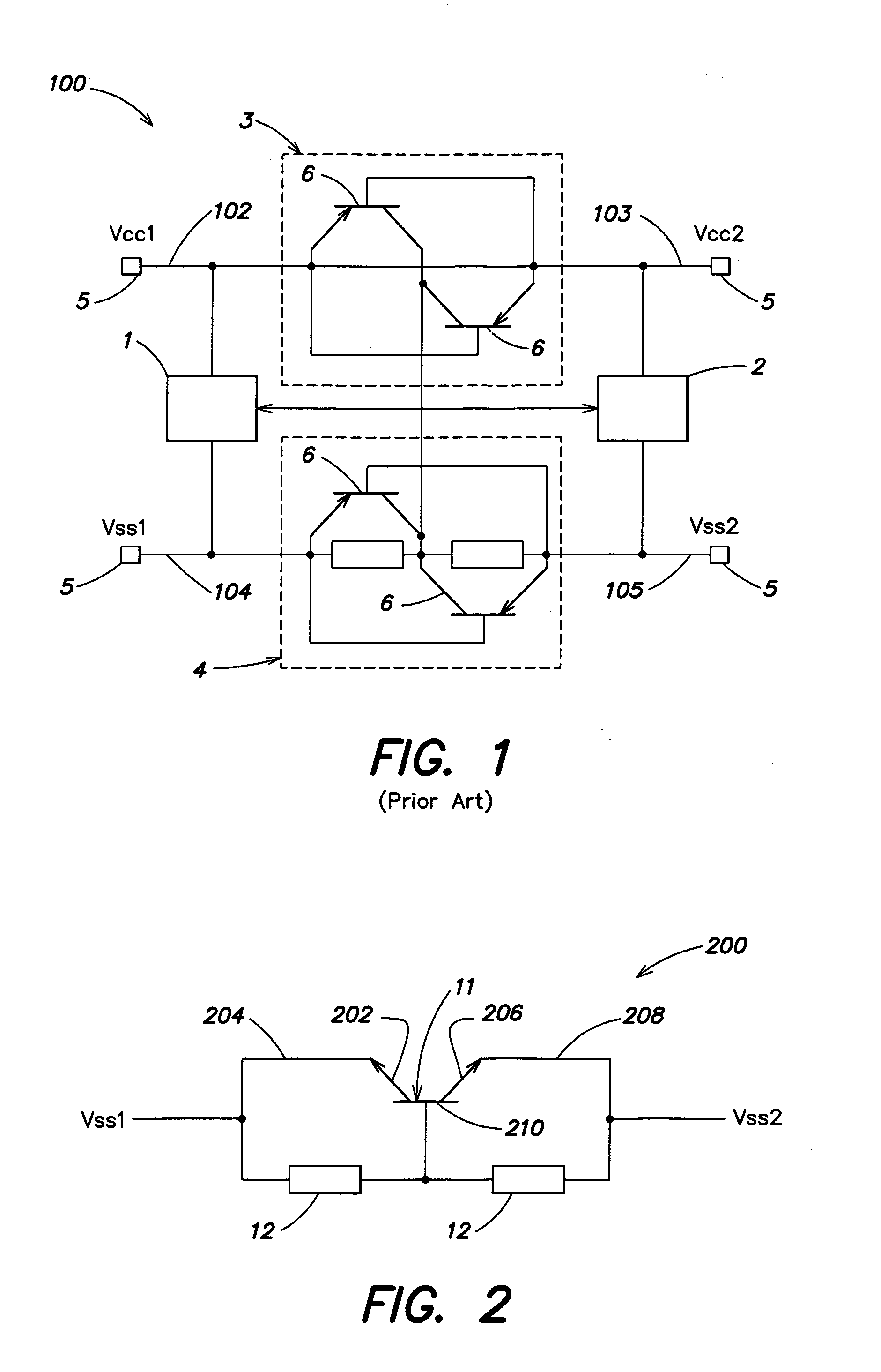
[0026]FIG. 2 is a schematic diagram illustration of a coupling circuit 200, which is an improvement to the prior art coupling circuit 100 of FIG. 1. The coupling circuit 200 includes an NPN transistor 11, the geometry and doping of which are symmetrical. The transistor 11 includes a first emitter 202 that is connected on a line 204 to a first voltage potential Vss1, and a second emitter 206 that is connected on a line 208 to a second voltage potential Vss2. The two power supply potentials Vss1, Vss2 are each connected through identical resistances 12 to a transistor base 210.

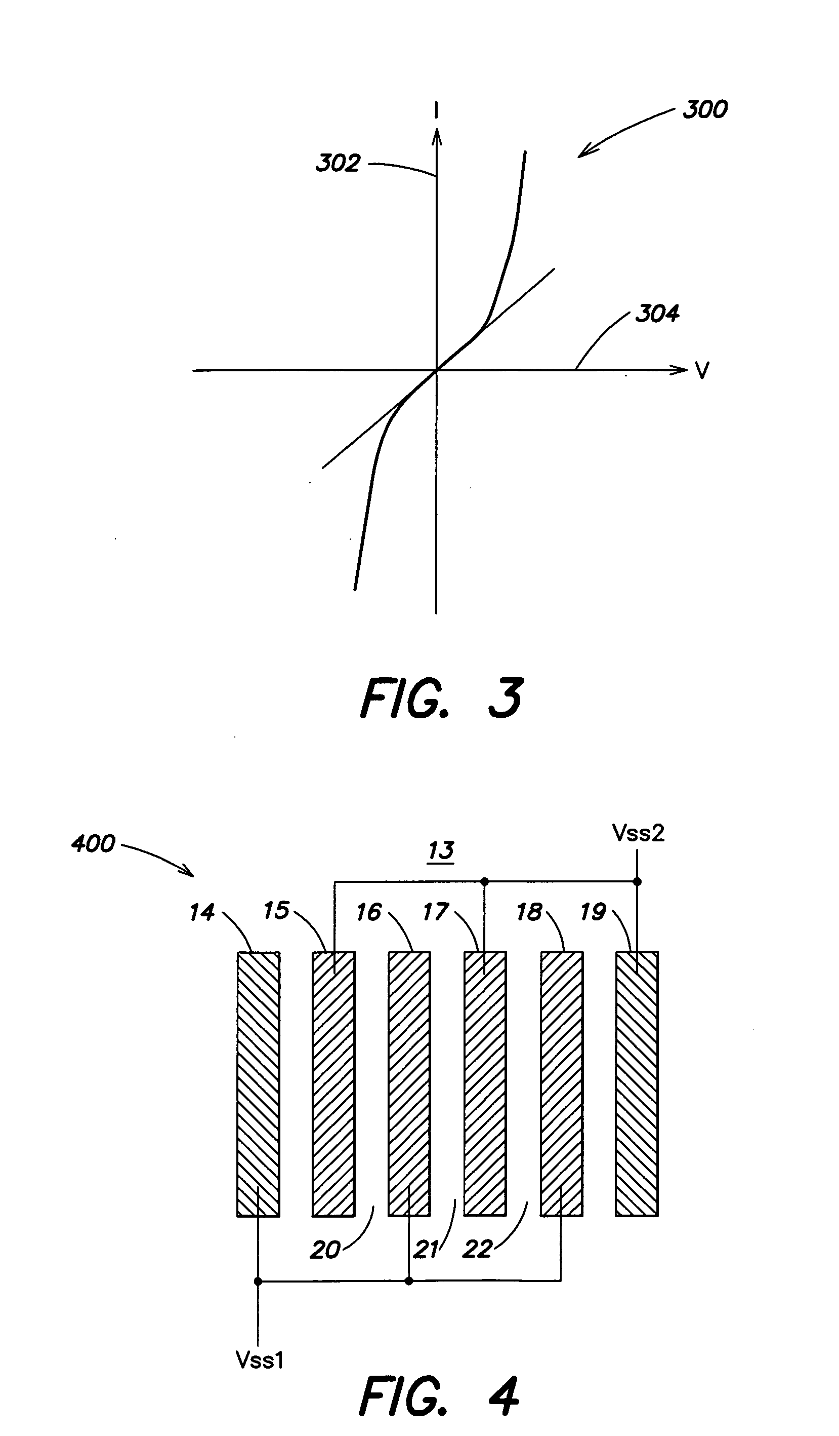
[0027]FIG. 3 is a plot 300 of the current-voltage characteristic of the coupling circuit illustrated in FIG. 2. Current is plotted along the vertical axis 302 and voltage is plotted along the horizontal axis 304. In response to small differences between the two power supply potentials, the behavior is resistive and is determined by the resistances 12 (FIG. 2). The activity of the transistor 11 is activated in re...


PUM


Abstract

An integrated circuit includes at least two circuit components formed on a common semiconductor substrate. Each circuit component has a self-contained supply voltage system. Coupling circuits couple the supply voltage systems for the at least two circuit components. Each coupling circuit includes at least one transistor having a base formed by or within the substrate itself; more specifically, by or within a region of the substrate contiguous with collector doping zones and emitter doping zones of the transistor. The resistance between the transistor base and the potentials of the two supply voltage systems coupled by each of the coupling circuits is the intrinsic resistance of the substrate between the region forming the base and one of each contact doping zone conductively connected to the collector or emitter through a metallization applied to the substrate. To obtain an identical coupling behavior for the transistor in both directions, the collector and emitter of the transistor are preferably symmetrical, i.e., a transistor with a double emitter. The coupling circuit may be implemented with a single transistor, the dimensions of which are fixed by the desired volume resistivity. Greater flexibility of design with respect to accommodating the coupling circuit on one substrate surface without an increased area requirement is provided by employing multiple transistors as the coupling circuit. These transistors may be distributed independently of each other on the substrate surface.

Description

BACKGROUND OF THE INVENTION[0001]The present invention relates to the field of integrated circuits, and in particular to integrated circuits that include at least two circuit components that are formed on a common semiconductor substrate and which each have self-contained supply voltage systems.[0002]Integrated circuits may include at least two circuit components that are formed on a common semiconductor substrate and which each have self-contained supply voltage systems. In addition, each of the two circuit components may include self-contained bonding spots for receiving an externally supplied voltage. Separate supply voltage systems of this type may be necessary to meet EMC requirements. In conventional technologies for highly integrated circuits, the semiconductor substrate is p-conductive and is connected to the power supply nodes of the two circuit components that carry the lowest voltage potential (e.g., “Vss”) among the applied potentials, such that the Vss potentials of the...

Claims


Application Information

Patent Timeline
Patent Type & Authority Patents(United States)
IPC IPC(8): H01L23/62H01L27/04H01L21/822H01L21/8222H01L23/48H01L27/02H01L27/06H01L27/082
CPCH01L27/0259H01L23/62
Inventor CZECH, MARTINREINHARD, ERWE
Owner MICRONAS
Why Eureka
Try Eureka