On-demand clock switching

a clock circuit and clock technology, applied in the direction of generating/distributing signals, instruments, sustainable buildings, etc., can solve the problems of electrical power consumption of fcbs, become more difficult, etc., and achieve the effect of reducing the power consumption mode of operation

Active Publication Date: 2007-04-10
SYNOPSYS INC
View PDF5 Cites 15 Cited by
  • Summary
  • Abstract
  • Description
  • Claims
  • Application Information

AI Technical Summary

Benefits of technology

[0006]In accordance with the invention there is provided a computing device comprising: a clock circuit for generating a first clock signal and a second clock signal; a first sub functional block (SFB) having an input port for receiving the first clock signal; a first functional circuit block (FCB) including the first SFB and for operating in accordance with predetermined parameters, the first FCB having a clock control port for providing a first clock control signal and a first clock signal input port for receiving a switchably coupled second clock signal, the first FCB having a circuitry portion for operating in one of a normal mode of operation and in a reduced power consumption mode of operation in dependence upon the switchably coupled second clock signal; and, a first clock control circuit for receiving the second clock signal and for switchably coupling the second clock signal to the first clock signal input port in dependence upon the first clock control signal.
[0007]In accordance with the invention there is provided a method of controlling power consumption: providing a first FCB for processing data using a first clock signal provided by a first clock circuit; providing a second FCB for processing data using a second clock signal provided by a second clock circuit; receiving a FCB control signal by the first FCB and the second FCB; determining whether the FCB control signal is for operating of at least one of the first FCB and the second FCB in one of a normal mode of operation and a reduced power consumption mode of operation; and, performing one of enabling of at least one of the first clock circuit and a second clock circuit in dependence upon whether at least one of the first FCB and the second FCB are for operating in the normal mode of operation and varying a frequency of at least one of the first clock circuit and a second clock circuit in dependence upon whether at least one of the first FCB and the second FCB are for operating in the normal mode of operation.
[0008]In accordance with the invention there is provided a method comprising: providing a first functional circuit block (FCB) for processing of data using a first clock circuit; providing a second FCB for processing of data using a second clock circuit; and, switchably enabling and disabling the first and second clock circuits independently in dependence upon performance requirements of the first and second FCBs.
[0009]In accordance with the invention there is provided a storage medium comprising instruction data stored thereon, the instruction data comprising: first instruction data for providing a first functional circuit block (FCB) for processing of data using a first clock circuit; second instruction data for providing a second FCB for processing of data using a second clock circuit; and, third instruction data for switchably enabling and disabling the first and second clock circuits independently in dependence upon performance requirements of the first and second FCBs.
[0010]In accordance with the invention there is provided a storage medium comprising instruction data stored thereon, the instruction data comprising: first instruction data for providing a first FCB for processing data using a first clock signal provided by a first clock circuit; second instruction data for providing a second FCB for processing data using a second clock signal provided by a second clock circuit; third instruction data for receiving a FCB control signal by the first FCB and the second FCB; fourth instruction data for determining whether the FCB control signal is for operating of at least one of the first FCB and the second FCB in one of a normal mode of operation and a reduced power consumption mode of operation; and, fifth instruction data for performing one of enabling of at least one of the first clock circuit and a second clock circuit in dependence upon whether at least one of the first FCB and the second FCB are for operating in the normal mode of operation and varying a frequency of at least one of the first clock circuit and a second clock circuit in dependence upon whether at least one of the first FCB and the second FCB are for operating in the normal mode of operation.

Problems solved by technology

For instance, cellular telephones have become widespread, but in order for their continued usefulness they must be able to operate for longer periods of time; an issue that becomes more difficult when an ever increasing number of features are integrated therein, such as, for example, color LCD video displays, or encryption processes.
Furthermore, FCBs coupled to the clock circuit receive the clock signal and gating circuitry within these FCBs consumes electrical power in response to the clock signal activating the gating circuitry.

Method used


Image

  • On-demand clock switching
  • On-demand clock switching
  • On-demand clock switching

Examples


Embodiment Construction

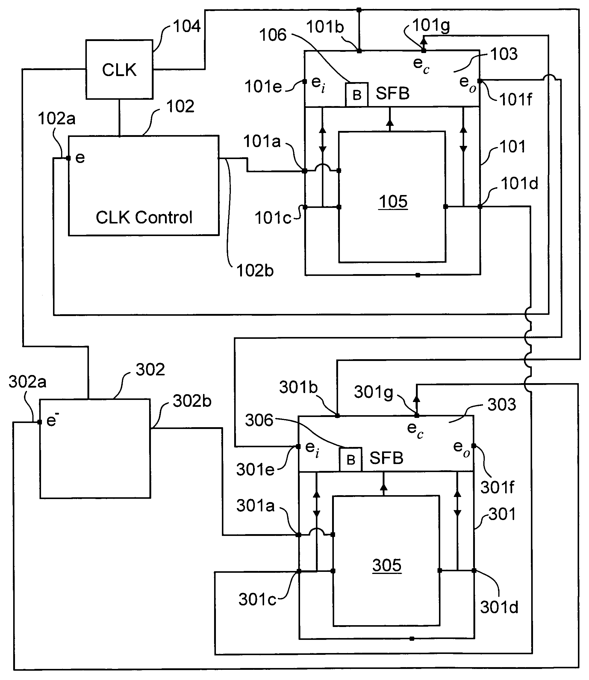
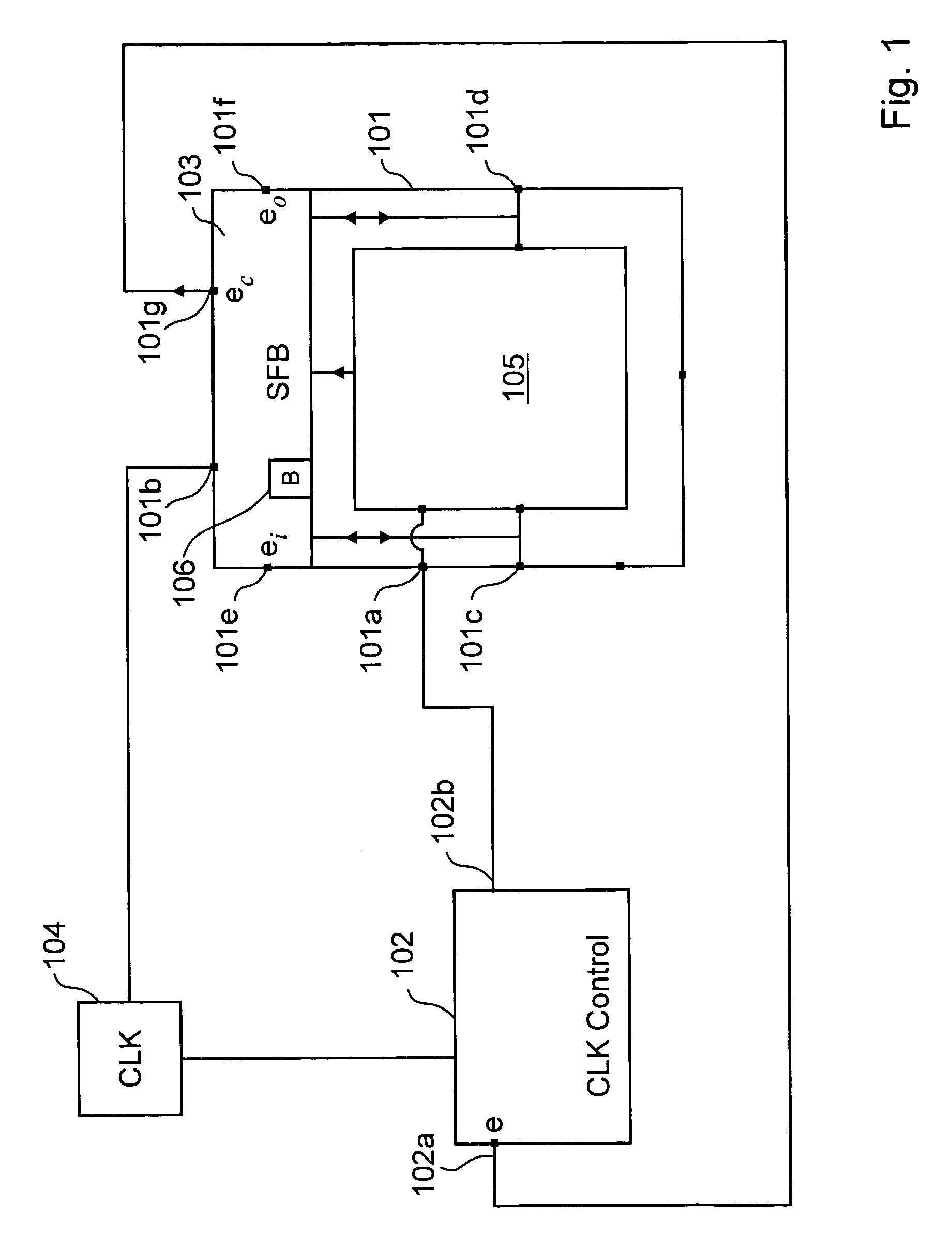
[0021]FIG. 1 illustrates an electrical circuit 100 comprised of a FCB 101, a clock control circuit 102 and a clock circuit 104. A sub-functional block (SFB) 103 is preferably disposed within the FCB 101 for implementing a clock control strategy. Additionally within the FCB 101 there is disposed a data processing block (DPB) 105 that is comprised of a majority of the internal circuitry of the FCB 101.

[0022]The clock circuit 104 provides a second clock signal to the clock control circuit 102 and a first clock signal to a SFB clock input port 101b disposed on the FCB 101. The first clock signal received on the SFB clock input port 101b is only for being received by circuitry forming the SFB 103. A FCB switched clock input port 101a is disposed on the FCB 101 for receiving of the switched second clock signal from an output port 102b of the clock control circuit 102. The switched second clock signal is for being received by the DPB 105 disposed within the FCB 101. A clock control port 10...


PUM


Abstract

First and second functional circuit blocks (FCBs) control the operation of a clock circuits coupled thereto in dependence upon processing requirements of the FCBs as well as power consumption considerations. When the FCB is not processing data, the clock circuit coupled to that FCB has one of its clock signal frequency reduced or is disabled so that the FCB consumes significantly reduced amounts of electrical power. Through controlling clock frequency and enabling and disabling of the clock circuit, electrical power consumption of the FCB is advantageously reduced.

Description

[0001]This patent application claims benefit from U.S. Provisional Application No. 60 / 458,004 filed on Mar. 28, 2003.FIELD OF THE INVENTION[0002]The invention relates to the area of power consumption of electrical circuits and more specifically in the area of controlling operation of clock circuits in order to control the power consumption of the electrical circuits.BACKGROUND OF THE INVENTION[0003]Circuits used in electrical devices are typically designed from functional circuit blocks (FCBs), where each of these blocks is designed to carry out predetermined processes within the electrical device. Power consumption plays an increasingly important role in modem devices that are being provided with increased functionality, but must maintain sufficient battery longevity in order for them to be sufficiently useful between battery recharge operations. For instance, cellular telephones have become widespread, but in order for their continued usefulness they must be able to operate for lo...

Claims


Application Information

Patent Timeline
Patent Type & Authority Patents(United States)
IPC IPC(8): G06F1/28G06F1/04G06F1/06G06F1/08G06F1/32
CPCG06F1/3203G06F1/324G06F1/3287Y02B60/1282Y02B60/1217Y02D10/00
Inventor HAMILTON, NEIL
Owner SYNOPSYS INC
Why Eureka
Try Eureka