
Analytical chip, analytical-chip unit, and analysis apparatus

a technology applied in the field of analytical chips and analytical chips, can solve the problems of requiring a great deal of labor for extraction or synthesis, a long time, etc., and achieve the effects of high precision, easy making of analytical chips with a fixed substance, and efficient analysis of fluid samples

Inactive Publication Date: 2007-04-17
MITSUBISHI CHEM CORP
View PDF19 Cites 57 Cited by
  • Summary
  • Abstract
  • Description
  • Claims
  • Application Information

AI Technical Summary

Benefits of technology

"The present invention provides an analytical chip with a flow channel for analyzing fluid samples. The chip has a closed shape and is divided into inner and outer flow channels. The chip also includes a projection member that divides the flow channel and inner flow channels. The chip can be easily made with a fixed specific substance according to a method involving the steps of fixing the intermediate plate, injecting the fluid sample, and adding the cover member. The chip can also have a basal plate, cover member, and intermediate plate with inner flow channels divided by partition walls. The chip can be used for various analytical purposes such as detecting specific substances in a fluid sample."

Problems solved by technology

Some of these products can be extracted or synthesized only in a restricted amount, or require a great deal of labor for extraction or synthesis.
It may take a long time, however, until the whole fluid sample has come into contact with the specific substances.

Method used


Image

  • Analytical chip, analytical-chip unit, and analysis apparatus
  • Analytical chip, analytical-chip unit, and analysis apparatus
  • Analytical chip, analytical-chip unit, and analysis apparatus

Examples


first embodiment

(1) First Embodiment

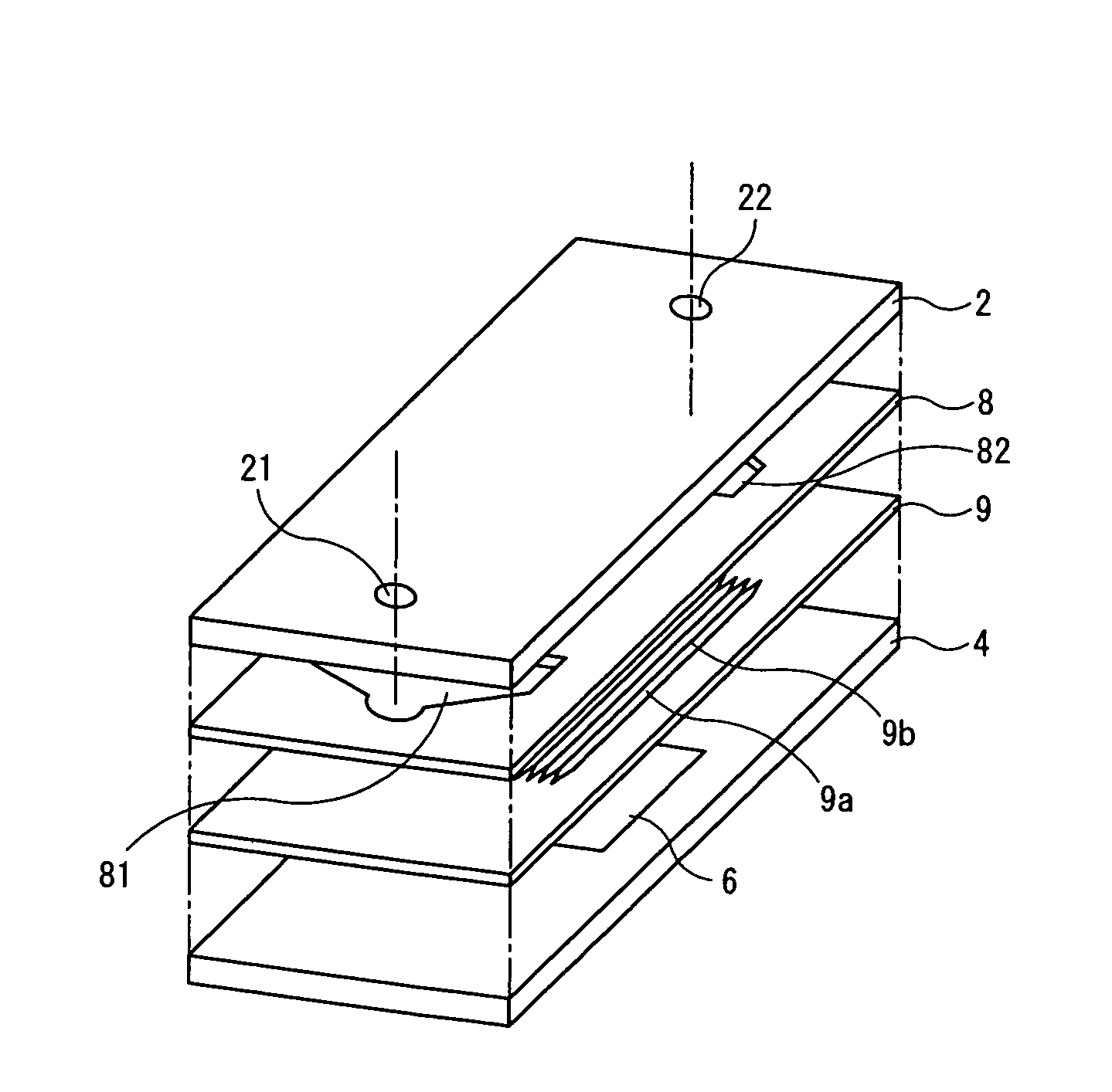
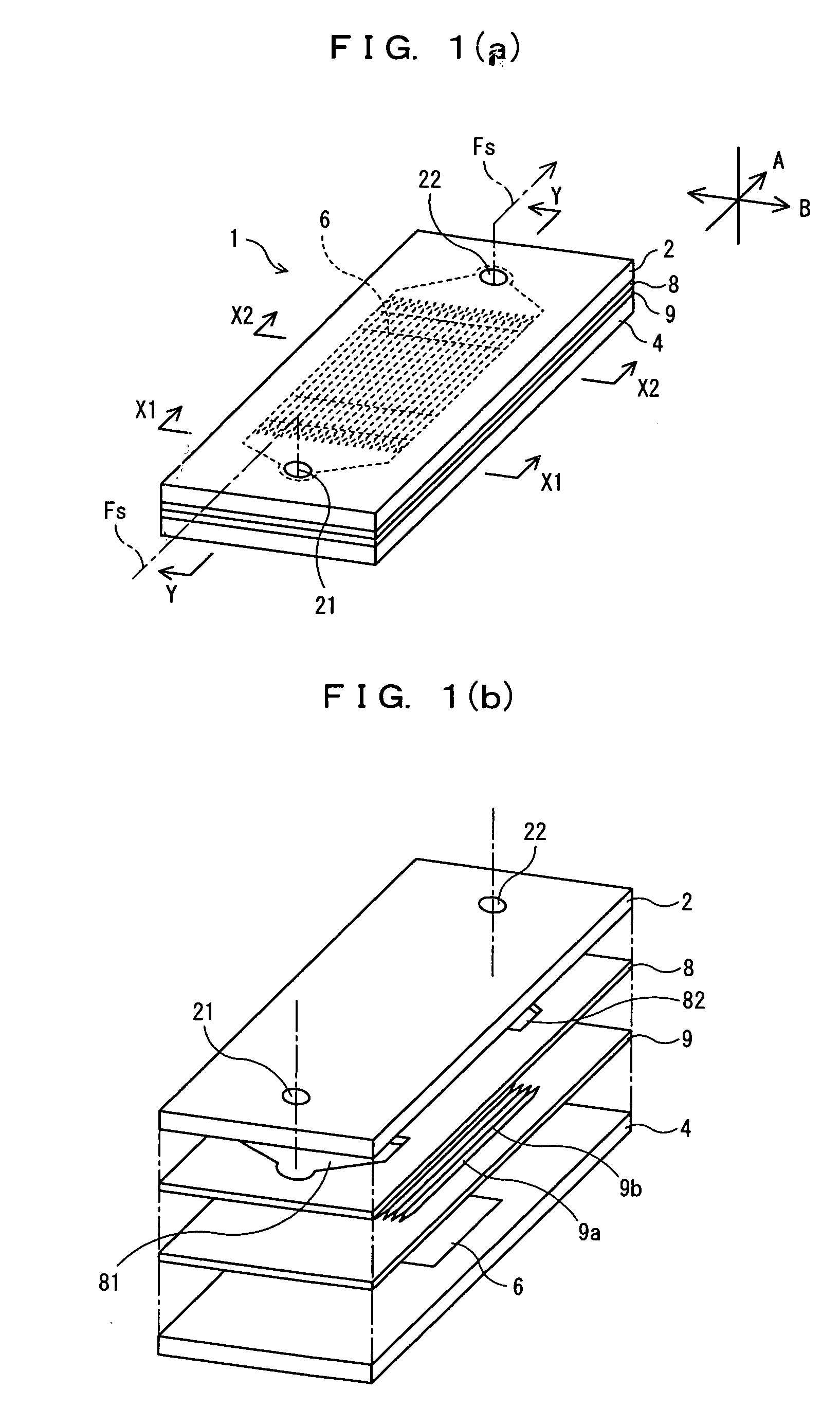
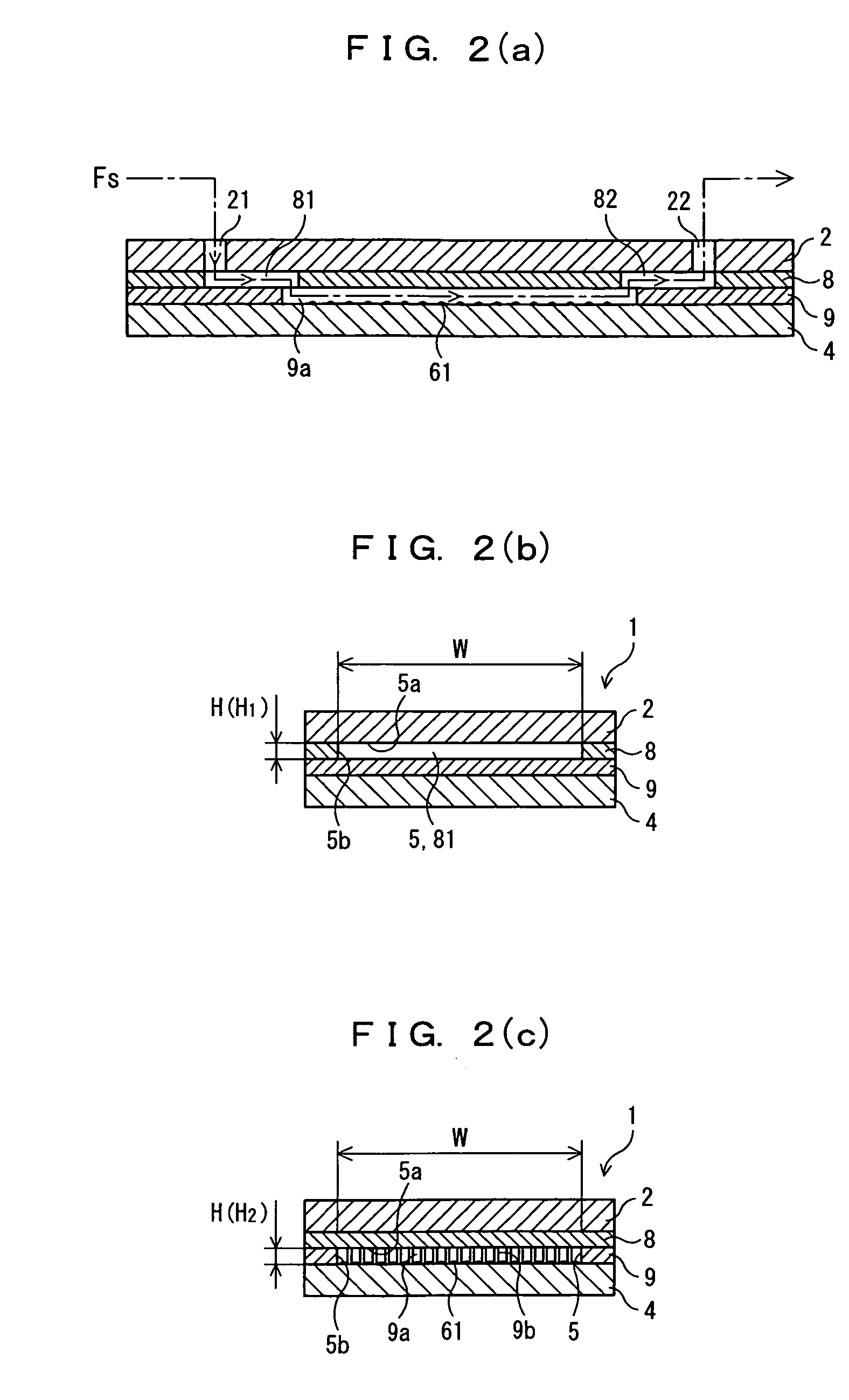
[0166]FIGS. 1–3 show analytical chip according to the first embodiment of the present invention. Specifically, FIG. 1(a) is a diagrammatic assembled perspective view of the chip, FIG. 1(b) is a diagrammatic exploded perspective view of the chip, FIG. 2(a) is a sectional view taken along line Y—Y of FIG. 1(a), FIG. 2(b) is a sectional view taken along line X1—X1 of FIG. 1(a), FIG. 2(c) is a sectional view taken along line X2—X2 of FIG. 1(a), FIG. 3(a) is a top view of the cover member of the chip, FIG. 3(b) is a top view of the first plate of the chip, FIG. 3(c) is a top view of the second plate of the chip, and FIG. 3(d) is a top view of the basal plate of the chip. In the following description, flow direction A of fluid sample Fs is defined as the major direction in which most of the fluid sample Fs flows through the flow channel. To take FIG. 4 as an example, the flow direction of flow channel 5′ is defined as the direction indicated by the arrow in solid line....

second embodiment

(2) Second Embodiment

[0259]An analytical chip according to the second embodiment of the present invention is constituted as an analytical chip (hereinafter called simply “the sensor chip”) used for an SPR sensor, based on surface plasmon resonance (SPR: surface plasmon resonance).

[0260]The following description will be made on the SPR sensor and the sensor chip with reference to FIGS. 10 and 11.

[0261]FIGS. 10 and 11 each show the second embodiment of the present invention. Specifically, FIG. 10 is a diagrammatic system block diagram of the SPR sensor, and FIG. 11 is a diagrammatic exploded perspective view of the sensor chip for assistance in explaining the constitution of the sensor chip. In FIGS. 10 and 11, the same or similar components as already explained in the first embodiment are designated by like reference characters to omit redundant explanations.

[0262]As shown in FIG. 10, the SPR sensor is composed of sensor chip 1A, light source 100 for irradiating the sensor chip 1A wi...

third embodiment

(3) Third Embodiment

[0279]FIGS. 12 through 14 each illustrate the constitution of an analytical chip according to the third embodiment of the present invention. Specifically, FIG. 12(a) is a diagrammatic assembled perspective view of the chip, FIG. 12(b) is a diagrammatic exploded perspective view of the chip, FIG. 13 is a diagrammatic bottom view of a plate of the chip, FIG. 14(a) is a sectional view taken from Y1—Y1 of FIG. 12(a), and FIG. 14(b) is a sectional view taken from X3—X3 of FIG. 12(a). The same or similar components as already explained in the first embodiment are designated by like reference characters to omit redundant explanations.

[0280]As shown in FIGS. 12(a), (b), the present analytical chip (hereinafter also called simply “the chip”) 1B is composed of cover member 2, plate 10, and basal plate 4.

[0281]A feature of the present analytical chip 1 compared to the first embodiment is that it has the plate (intermediate plate) 10 instead of the plates 8, 9. Hence, the fo...


PUM

PropertyMeasurementUnit
cross sectional areaaaaaaaaaaa
aspect ratioaaaaaaaaaa

Abstract

An analytical chip is provided with a flow channel (5), whose section is in a closed shape and through which a fluid sample (Fs) is made to flow, for carrying out analysis regarding the fluid sample (Fs) based on interaction between a predetermined substance and a specific substance (61), which is placed facing said flow channel (5). The chip further has a projection member (9b) attached to said flow channel (5). With this arrangement, it becomes possible to analyze the fluid sample (Fs) efficiently with high precision.

Description

CROSS-REFERENCE TO RELATED APPLICATION[0001]This application is a continuation of International Application PCT / JP2003 / 08851 filed on Jul. 11, 2003, now pending and claims priority from Japanese Patent Application 2002-204677 filed on Jul. 12, 2002, the contents of which are herein wholly incorporated by reference.TECHNICAL FIELD[0002]The present invention relates to a chip provided with a flow channel, through which a fluid sample is made to flow, and used for analyzing the fluid sample, and also relates to a chip unit, an analysis apparatus and method using the chip, and a method of making the chip.BACKGROUND ART[0003]Various techniques have been proposed until now for detecting the reaction or binding between a fluid sample and a substance fixed to a chip and for carrying out different kinds of analyses rapidly within a limited time, and some of those have been already put into practical use as high throughput analysis systems.[0004]Among those techniques, attention has been give...

Claims


Application Information

Patent Timeline
Patent Type & Authority Patents(United States)
IPC IPC(8): G01F1/68B01F5/06B01F13/00B01L3/00C40B40/06C40B40/10G01N30/00G01N33/543
CPCB01F5/0646B01F13/0059B01L3/502707B01L3/502746G01N30/0005G01N33/54366B01F5/0655B82Y35/00B01J2219/00497B01J2219/00549B01J2219/00574B01J2219/00576B01J2219/00585B01J2219/00596B01J2219/00605B01J2219/00612B01J2219/00637B01J2219/00641B01J2219/00659B01J2219/00707B01J2219/00722B01J2219/00725B01L3/502723B01L2300/0636B01L2300/0825B01L2300/0864B01L2300/0867B01L2300/0877B01L2300/0887B01L2400/086B82Y30/00C40B40/06C40B40/10G01N30/6043G01N30/6065G01N30/466G01N30/461B01F25/433B01F25/4338B01F33/30
Inventor TAKAYAMA, HIDEHITO
Owner MITSUBISHI CHEM CORP
Learn More