Method of forming a self-aligned contact structure using a sacrificial mask layer

a contact structure and self-aligning technology, applied in the field of self-aligning contact structure using a sacrificial mask layer, can solve the problems of device failure, weak structural strength of fabricated semiconductor devices, and disadvantages of conventional techniques described above, so as to prevent shorts or breakdown voltage decreases, reduce contact plug height, and prevent etching damage of top surfaces

Active Publication Date: 2007-04-17
SAMSUNG ELECTRONICS CO LTD
View PDF4 Cites 13 Cited by
  • Summary
  • Abstract
  • Description
  • Claims
  • Application Information

AI Technical Summary

Benefits of technology

[0019]Embodiments of the invention provide a method of forming a self-aligned contact structure, the method being capable of lowering a height of a contact plug and preventing etching damages of top surfaces of interconnections as well as preventing shorts or breakdown voltage decreases between the interconnections and the plug.
[0020]These embodiments provide a method of forming a self-aligned contact structure, the method being capable of reducing a coupling capacitance between the interconnections.

Problems solved by technology

However, the conventional technique described above has disadvantages as well, as described below.
The exposed interconnections 35 short with the plugs 85, and may cause a device failure.
Further, in such cases, aspect ratios of the contact holes 75 increase, and the fabricated semiconductor device is structurally weak because the increased total height of the device.

Method used


Image

  • Method of forming a self-aligned contact structure using a sacrificial mask layer
  • Method of forming a self-aligned contact structure using a sacrificial mask layer
  • Method of forming a self-aligned contact structure using a sacrificial mask layer

Examples


Embodiment Construction

[0027]Hereinafter, the present invention will be described in detail by describing preferred embodiments thereof with reference to the accompanying drawings. Like reference numerals refer to like elements throughout the drawings.

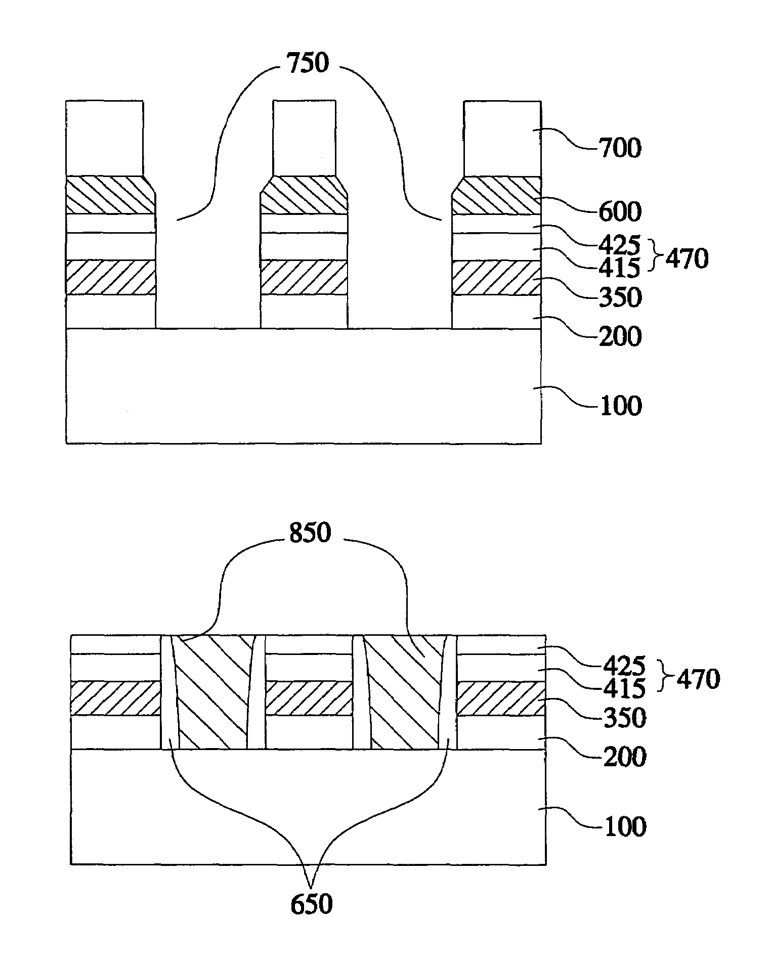
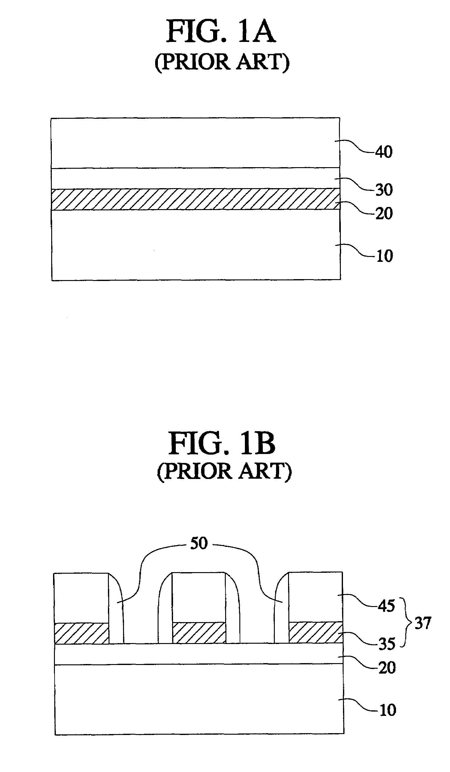
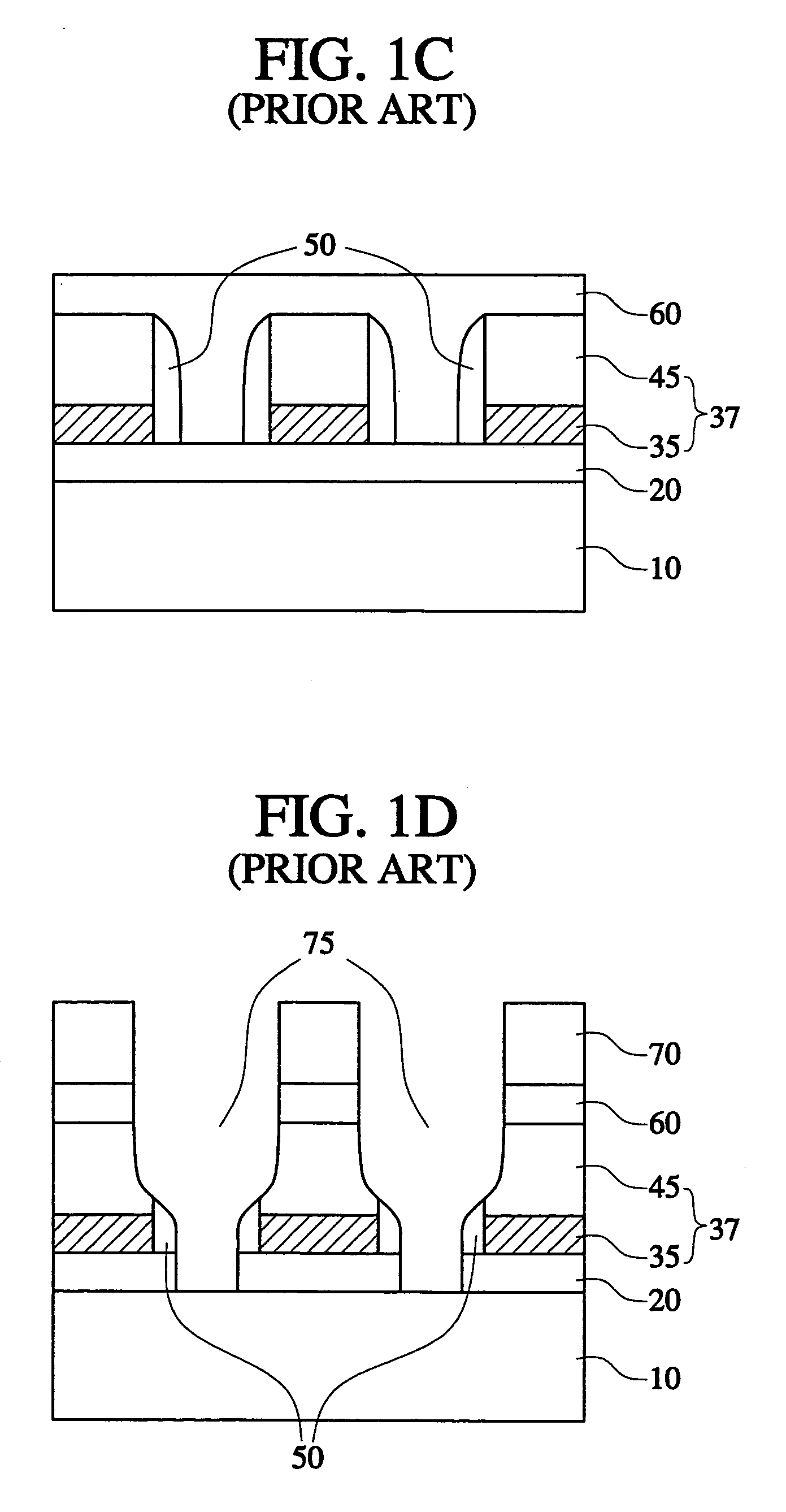
[0028]FIGS. 2A to 2G are cross-sectional diagrams illustrating a method of forming a self-aligned contact structure in accordance with an embodiment of the present invention. Referring to FIG. 2A, a lower insulating layer 200 is formed on a semiconductor substrate 100. The semiconductor substrate 100 may have active regions (not shown) or conductive pads (not shown) therein for electrical connections to be formed thereto. When the active regions are exposed on the surface of the semiconductor substrate 100, the lower insulating layer 200 may serve as a gate dielectric layer.

[0029]The lower insulating layer 200 may be formed of an oxide layer or a nitride layer, for example. When the lower insulating layer 200 serves as a gate dielectric layer, it is preferab...


PUM


Abstract

Disclosed is a method of forming a self-aligned contact structure using a sacrificial mask layer. The method includes forming a plurality of parallel interconnection patterns on a semiconductor substrate. Each of the interconnection patterns has an interconnection and a mask pattern, which are sequentially stacked. Interlayer insulating layer patterns are formed to fill gap regions between the interconnection patterns. The mask patterns are partially etched to form recessed mask patterns that define grooves between the interlayer insulating layer patterns. Then, sacrificial mask patterns filling the grooves are formed. A predetermined region of the interlayer insulating layer patterns is etched using the sacrificial mask patterns as etching masks to form a self-aligned contact hole that exposes a predetermined region of the semiconductor substrate. A spacer is formed of a sidewall of the self-aligned contact hole, and a plug surrounded by the spacer is formed in the self-aligned contact hole.

Description

[0001]This application claims priority from Korean Patent Application No. 2003-0033863 filed on May 27, 2003, the entire contents of which are hereby incorporated by reference.BACKGROUND OF THE INVENTION[0002]1. Field of the Invention[0003]This disclosure relates to a method of fabricating a semiconductor device, and more particularly a method of forming a self-aligned contact structure using a sacrificial mask layer.[0004]2. Description of the Related Art[0005]As integrated circuit devices become more highly integrated, the width of interconnections and spacing between interconnections have also been reduced. Self-aligned contact technology has been used to increase alignment margins when using a photolithography technique to form contact holes in predetermined regions between the interconnections.[0006]FIG. 1A to FIG. 1E are cross-sectional diagrams illustrating a method of forming a self-aligned contact structure in accordance with a conventional technique.[0007]Referring to FIG....

Claims


Application Information

Patent Timeline
Patent Type & Authority Patents(United States)
IPC IPC(8): H01L21/44H01L23/52H01L21/28H01L21/60H01L21/768
CPCH01L21/76897H01L2924/3011H01L2924/0002H01L2924/00H01L21/28
Inventor YUN, CHEOL-JUCHUNG, TAE-YOUNG
Owner SAMSUNG ELECTRONICS CO LTD
Why Eureka
Try Eureka