HDP-CVD multistep gapfill process

a multi-step, gapfilling technology, applied in the direction of solid-state diffusion coating, fluid pressure measurement, chemical vapor deposition coating, etc., can solve the problems of increasing the aspect ratio, progressively more difficult to fill the gap without leaving voids, affecting the operation of the completed device, etc., to achieve the effect of reducing the average molecular weight and reducing the sputtering characteristics

Inactive Publication Date: 2007-04-17
APPLIED MATERIALS INC
View PDF93 Cites 111 Cited by
  • Summary
  • Abstract
  • Description
  • Claims
  • Application Information

AI Technical Summary

Benefits of technology

[0006]Embodiments of the invention thus provide a dep / etch / dep process in which a gap is filled with a first HDP-CVD deposition step, followed by an etching step, followed by a remainder HDP-CVD deposition step. The precursor gases used in each of the deposition steps may be similar and comprise a silicon-containing gas and an oxygen-containing gas to deposit a silicon oxide film for filling a gap in a surface of a substrate. The fluent gas during the remainder deposition has a lower average molecular weight than the fluent gas during the first deposition step. For example, the fluent gas during the first deposition step may comprise an inert gas and during the remainder deposition step may comprise H2. The higher average molecular weight of the fluent gas during the first deposition step provides some cusping over structures that define the gap to protect them during the etching step. The lower average molecular weight of the fluent gas during the remainder deposition step has reduced sputtering characteristics and is effective at filling the remainder of the gap.

Problems solved by technology

One of the persistent challenges faced in the development of semiconductor technology is the desire to increase the density of circuit elements and interconnections on substrates without introducing spurious interactions between them.
As circuit densities increase, however, the widths of these gaps decrease, increase their aspect ratios and making it progressively more difficult to fill the gaps without leaving voids.
The formation of voids when the gap is not filled completely is undesirable because they may adversely affect operation of the completed device, such as by trapping impurities within the insulative material.
The high reactivity of the species in the plasma reduces the energy required for a chemical reaction to take place, and thus lowers the temperature required for such CVD processes when compared with conventional thermal CVD processes.
Such dep / etch / dep processes have also been used with PECVD techniques, but some thermal and PECVD techniques are still unable to fill gaps having very large aspect ratios even by cycling deposition and etching steps.

Method used


Image

  • HDP-CVD multistep gapfill process
  • HDP-CVD multistep gapfill process
  • HDP-CVD multistep gapfill process

Examples


Embodiment Construction

1. Introduction

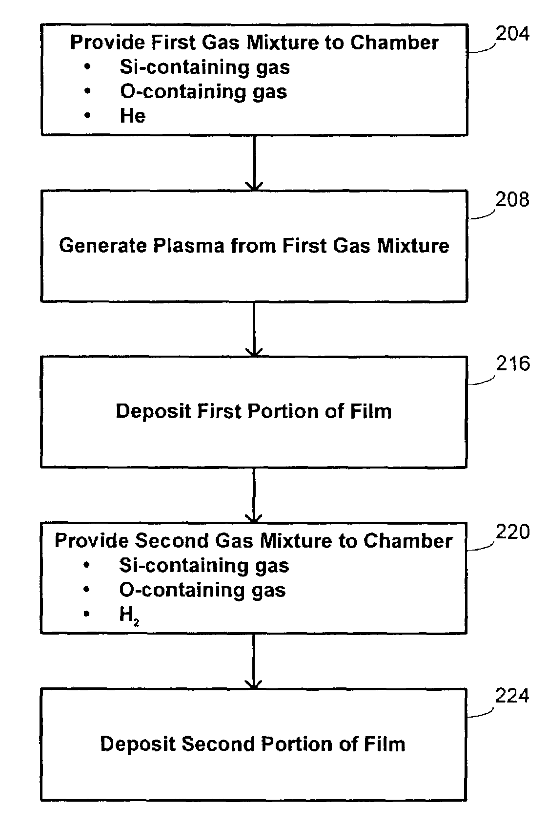
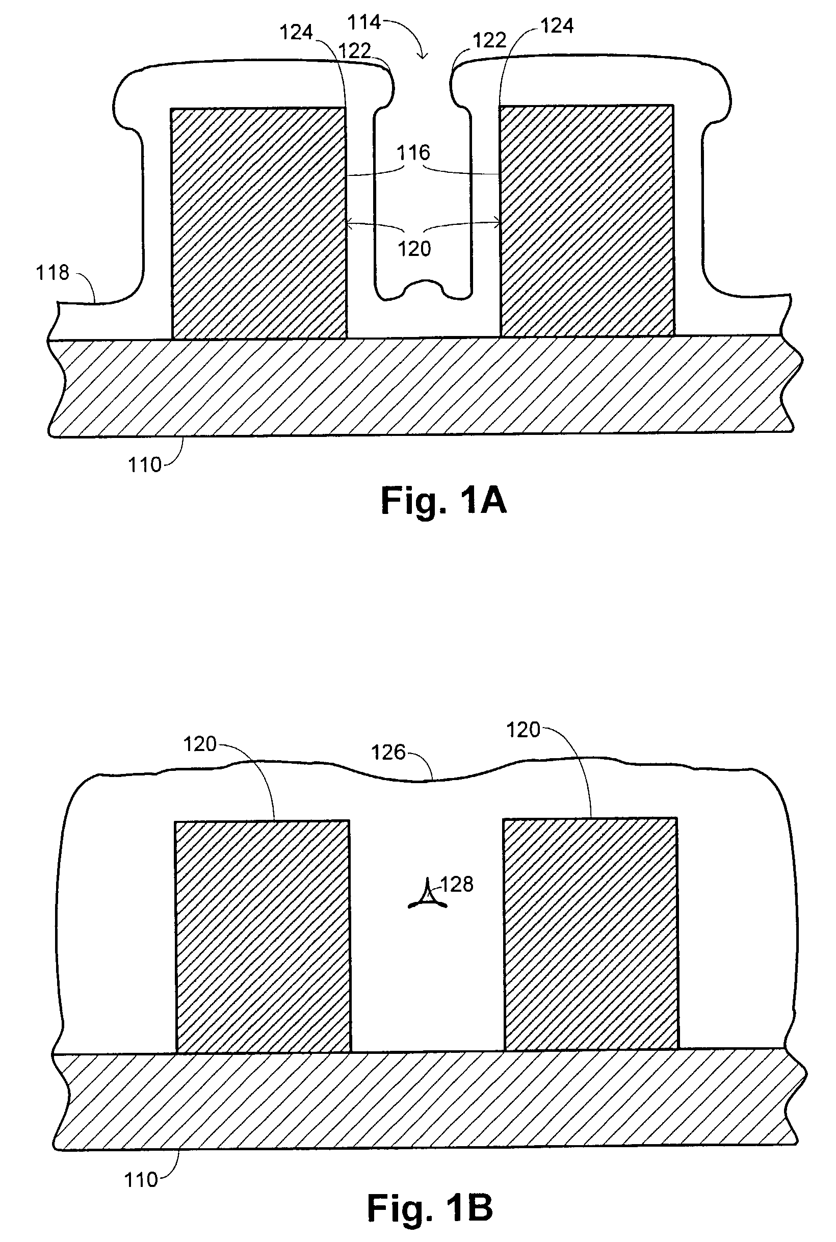
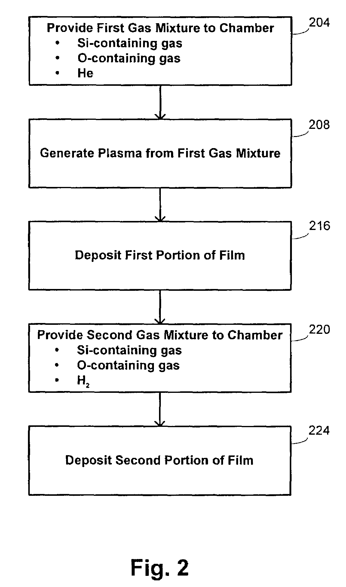
[0023]Embodiments of the invention are directed to methods and apparatus for depositing a film to fill a gap in a surface of a substrate. For gaps of a given width, these embodiments use a multistep deposition and etching process and exploit different sputtering characteristics of an HDP-CVD technique in different portions of the process. These different sputtering characteristics are achieved by the use of different fluent gases to provide the sputtering agent and also by adjusting flow rates of process gases to achieve different deposition-to-sputtering ratios. The combination of effects provided by the cycling of deposition and etching steps and by the variation in sputtering characteristics combine synergistically to permit substantially void-free filling of gaps having very high aspect ratios. In particular, the embodiments of the invention may be used for filling gaps in 100-nm technology (0.10 μm) and at least down to 65-nm technology (0.065 μm). The embodiment...


PUM

PropertyMeasurementUnit
wt. %aaaaaaaaaa
wt. %aaaaaaaaaa
temperatureaaaaaaaaaa

Abstract

A gapfill process is provided using cycling of HDP-CVD deposition, etching, and deposition step. The fluent gas during the first deposition step includes an inert gas such as He, but includes H2 during the remainder deposition step. The higher average molecular weight of the fluent gas during the first deposition step provides some cusping over structures that define the gap to protect them during the etching step. The lower average molecular weight of the fluent gas during the remainder deposition step has reduced sputtering characteristics and is effective at filling the remainder of the gap.

Description

BACKGROUND OF THE INVENTION[0001]One of the persistent challenges faced in the development of semiconductor technology is the desire to increase the density of circuit elements and interconnections on substrates without introducing spurious interactions between them. Unwanted interactions are typically prevented by providing gaps or trenches that are filled with electrically insulative material to isolate the elements both physically and electrically. As circuit densities increase, however, the widths of these gaps decrease, increase their aspect ratios and making it progressively more difficult to fill the gaps without leaving voids. The formation of voids when the gap is not filled completely is undesirable because they may adversely affect operation of the completed device, such as by trapping impurities within the insulative material.[0002]Common techniques that are used in such gapfill applications are chemical-vapor deposition (“CVD”) techniques. Conventional thermal CVD proce...

Claims


Application Information

Patent Timeline
Patent Type & Authority Patents(United States)
IPC IPC(8): C23C16/00C23C14/00C23C14/32C23C16/04C23C16/40C23C16/56C25B9/00C25B11/00H01LH01L21/30H01L21/311H01L21/316H01L21/768
CPCC23C16/045C23C16/401C23C16/56H01L21/02164H01L21/02274H01L21/31116H01L21/31612H01L21/76837
Inventor KARIM, M. ZIAULKAPOOR, BIKRAMWANG, ANCHUANLI, DONG QINGOZEKI, KATSUNARIVELLAIKAL, MANOJLI, ZHUANG
Owner APPLIED MATERIALS INC
Why Eureka
Try Eureka