Replacement gate process for making a semiconductor device that includes a metal gate electrode

a technology of metal gate electrodes and replacement gate processes, which is applied in the direction of semiconductor devices, basic electric elements, electrical equipment, etc., can solve the problems of inability to completely fill the trench with metal, inability to use replacement gate processes, and difficulty in uniform coating of the sidewalls of the resulting trench with various materials

Inactive Publication Date: 2007-04-24
INTEL CORP
View PDF39 Cites 129 Cited by
  • Summary
  • Abstract
  • Description
  • Claims
  • Application Information

AI Technical Summary

Problems solved by technology

Although such a profile may be suitable for processes that retain the patterned polysilicon layers, it may be inappropriate for a replacement gate process, especially when making transistors with 45 nm or smaller gate lengths.
After removing such a patterned polysilicon layer, it may be difficult to uniformly coat the sidewalls of the resulting trench with various materials.
In addition, it may not be possible to completely fill such a trench with metal, as voids may form at the trench center.

Method used


Image

  • Replacement gate process for making a semiconductor device that includes a metal gate electrode
  • Replacement gate process for making a semiconductor device that includes a metal gate electrode
  • Replacement gate process for making a semiconductor device that includes a metal gate electrode

Examples


Embodiment Construction

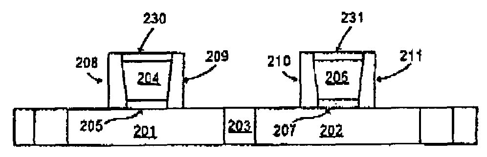
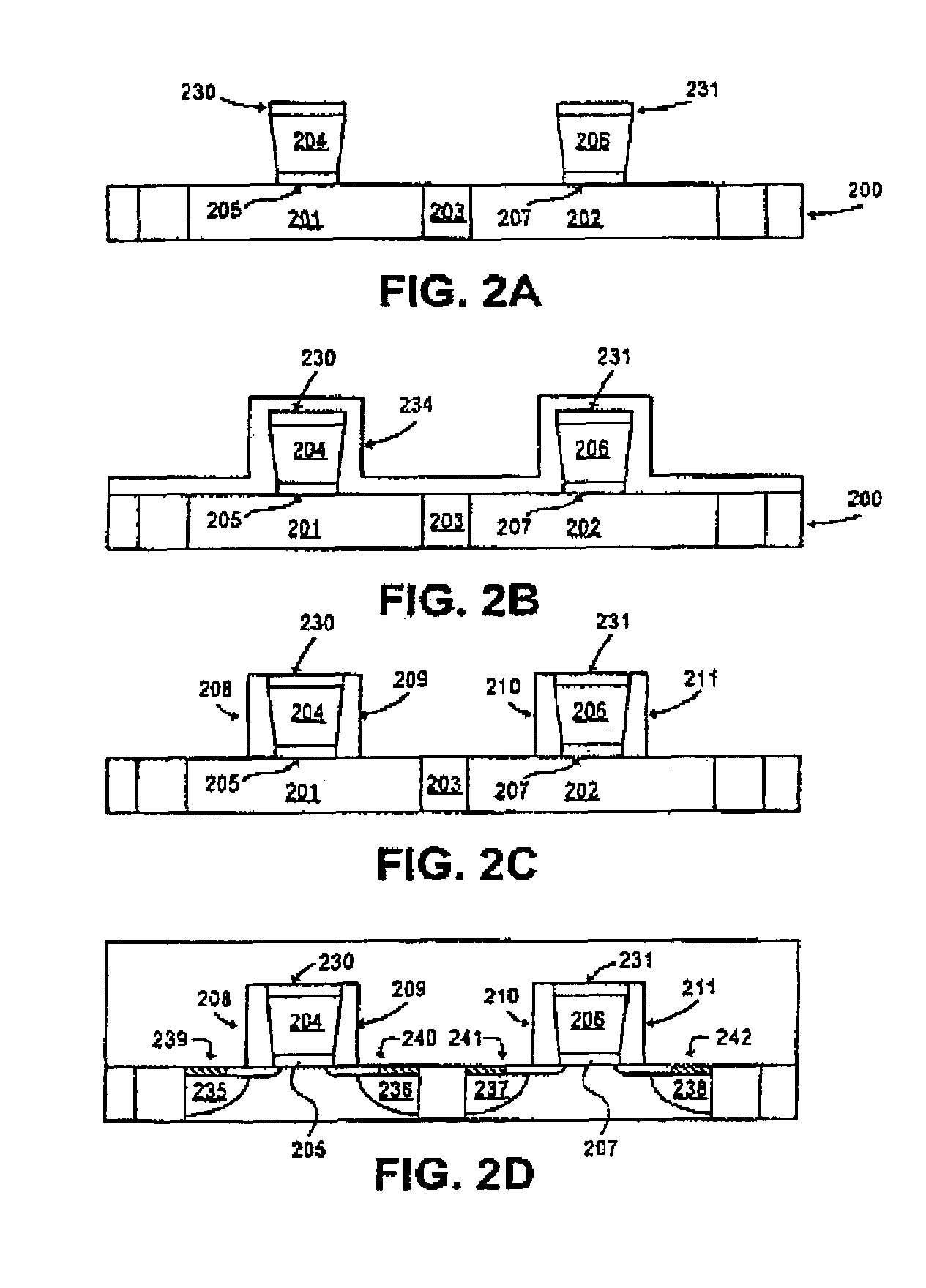
[0008]A method for making a semiconductor device is described. That method comprises forming a dielectric layer on a substrate, then forming a polysilicon layer on the dielectric layer. The polysilicon layer is then etched to generate a patterned polysilicon layer. That layer's upper surface is less than or equal to about 45 angstroms wide, and that layer's lower surface is less than or equal to about 40 angstroms wide. The upper surface is at least about 5 angstroms wider than the lower surface.

[0009]In the following description, a number of details are set forth to provide a thorough understanding of the present invention. It will be apparent to those skilled in the art, however, that the invention may be practiced in many ways other than those expressly described here. The invention is thus not limited by the specific details disclosed below.

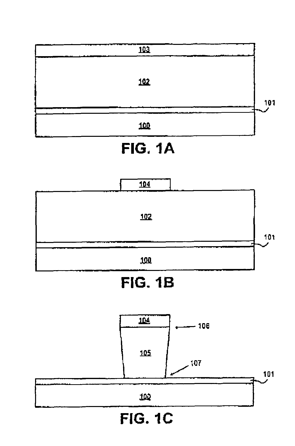
[0010]FIGS. 1A–1C illustrate structures that may be formed, when carrying out an embodiment of the method of the present invention. Initiall...


PUM


Abstract

A method for making a semiconductor device is described. That method comprises forming a polysilicon layer on a dielectric layer, which is formed on a substrate. The polysilicon layer is etched to generate a patterned polysilicon layer with an upper surface that is wider than its lower surface. The method may be applied, when using a replacement gate process to make transistors that have metal gate electrodes.

Description

FIELD OF THE INVENTION[0001]The present invention relates to methods for making semiconductor devices, in particular, semiconductor devices with metal gate electrodes.BACKGROUND OF THE INVENTION[0002]When making a CMOS device that includes metal gate electrodes, a replacement gate process may be used to form gate electrodes from different metals. In that process, a first polysilicon layer, bracketed by a pair of spacers, is removed to create a trench between the spacers. The trench is filled with a first metal. A second polysilicon layer is then removed, and replaced with a second metal that differs from the first metal.[0003]Current processes for etching polysilicon layers generate patterned polysilicon layers with side walls that are vertical or slightly inclined such that the lower surface of each patterned layer is wider than the upper surface. Although such a profile may be suitable for processes that retain the patterned polysilicon layers, it may be inappropriate for a replac...

Claims


Application Information

Patent Timeline
Patent Type & Authority Patents(United States)
IPC IPC(8): H01L21/8238H01L27/10H01L21/00H01L21/336H01L21/4763H01L21/84
CPCH01L21/84H01L29/66545H01L29/66772
Inventor SHAH, UDAYBARNS, CHRIS E.DOCZY, MARK L.BRASK, JUSTIN K.KAVALIEROS, JACKMETZ, MATTHEW V.CHAU, ROBERT S.
Owner INTEL CORP
Why Eureka
Try Eureka