Stacked semiconductor memory device

a memory device and semiconductor technology, applied in memory devices, basic electric elements, instruments, etc., can solve the problems of increasing power consumption of memory devices, and reducing the power consumption of three-dimensional semiconductor memory devices. , the effect of reducing the length of chip in-plane dq lines and the number of interchip interconnections

Active Publication Date: 2007-04-24
LONGITUDE LICENSING LTD
View PDF9 Cites 16 Cited by
  • Summary
  • Abstract
  • Description
  • Claims
  • Application Information

AI Technical Summary

Benefits of technology

[0014]The present invention was achieved in view of the above-described problems of the prior art and has as an object the provision of a three-dimensional semiconductor memory device that allows a reduction of the interconnection capacitance that is necessary for charging and discharging when transferring data between chips and that thus reduces power consumption of the memory device.
[0030]According to the present invention, in a three-dimensional semiconductor memory device in which memory cell array chips are stacked, the banks of a memory cell array may be divided sub-banks equal in number to the number of input / output bits and organized and arranged for each input / output bit. Connecting DQ lines from the sub-banks t to interchip interconnections for each input / output bit minimizes both the length of chip in-plane DQ lines and the number of interchip interconnections, whereby the interconnection capacitance can be reduced and the power consumption of the three-dimensional semiconductor memory device can be decreased.

Problems solved by technology

However, because there are limits to the miniaturization of semiconductors, new technologies are being sought to achieve further increases in the degree of integration.
Nevertheless, vias that are used in three-dimensional interchip interconnections have a problem of greater capacitance than ordinary in-plane interconnections.
This increase in interconnection capacitance raises the problem of increased power consumption of the memory device.

Method used


Image

  • Stacked semiconductor memory device
  • Stacked semiconductor memory device
  • Stacked semiconductor memory device

Examples


working example 1

[0043]FIG. 4 shows the configuration of the first working example of a stacked semiconductor memory device according to the present invention.

[0044]In the present working example, memory cell array chip 31, which is DRAM having a memory capacity of 512 Mb, is stacked on interface chip 30 on which integrated circuits are provided for interfacing with the outside. Memory cell array chip 31 has four input / output bits DQ0, DQ1, DQ2, and DQ3, and four banks BK0, BK1, BK2, and BK3.

[0045]Each bank is divided into four, which is the number of input / output bits. For example, bank BK0 is divided into the four sub-banks: BK0 (DQ0) that is composed of the memory cells of DQ0, BK0 (DQ1) that is composed of the memory cells of DQ1, BK0 (DQ2) that is composed of the memory cells of DQ2, and BK0 (DQ3) that is composed of the memory cells of DQ3. Banks BK1, BK2, and BK3 are similarly divided into the sub-banks BK1 (DQ0)-BK1 (DQ3), BK2 (DQ0)-BK2 (DQ3), and BK3 (DQ0)-BK3 (DQ3), respectively, resulting...

working example 2

[0050]The following explanation regards the second working example of the present invention with reference to FIG. 6. FIG. 6 shows the configuration of a three-dimensional semiconductor DRAM device. In the present working example, memory cell array chips 51 of DRAM having a memory capacity of 512 Mb are stacked on interface chip 50 in which interface circuits with the outside are integrated.

[0051]All of memory cell array chips 51 have the same configuration with four input / output bits DQ0, DQ1, DQ2, and DQ3, and four banks BK0, BK1, BK2, and BK3. Each bank is divided into four, which is the number of input / output bits. For example, bank BK0 is divided into the four sub-banks: BK0 (DQ0) that is composed of the memory cells of DQ0; BK0 (DQ1) that is composed of the memory cells of DQ1; BK0 (DQ2) that is composed of the memory cells of DQ2; and BK0 (DQ3) that is composed of the memory cells of DQ3. BK1 (DQ0)-BK1 (DQ3), BK2 (DQ0)-BK2 (DQ3), and BK3 (DQ0)-BK3 (DQ3) are similarly divided,...

working example 3

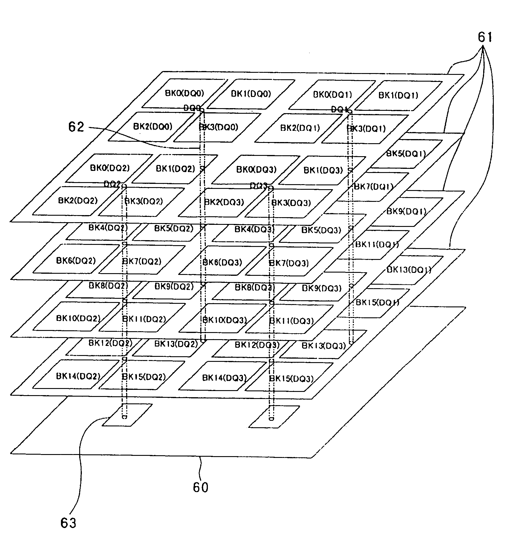
[0055]The following explanation regards the third working example of the present invention with reference to FIG. 7. FIG. 7 shows the configuration of a three-dimensional semiconductor DRAM device, which is the third working example of the present invention. In the present working example, four memory cell array chips 61 that are DRAM having a memory capacity of 512 Mb are stacked on interface chip 60, on which interface circuits that connect with the outside are integrated. Memory cell array chips 61 are composed of memory cell arrays having four input / output bits and four banks.

[0056]Although all memory cell array chips 51 have the same memory configuration in the second working example, in the present working example, the chips have four different banks on each chip. In other words, the memory configuration of the four stacked DRAM devices includes four input / output bits DQ0, DQ1, DQ2, and DQ3, and 16 banks from BK0–BK15. Each bank is then divided into four parts, which is the nu...


PUM


Abstract

A three-dimensional semiconductor memory device having the object of decreasing the interconnection capacitance that necessitates electrical charge and discharge during data transfer and thus decreasing power consumption is provided with: a plurality of memory cell array chips, in which sub-banks that are the divisions of bank memory are organized and arranged to correspond to input / output bits, are stacked on a first semiconductor chip; and interchip interconnections for connecting the memory cell arrays such that corresponding input / output bits of the sub-banks are the same, these interchip interconnections being provided in a number corresponding to the number of input / output bits and passing through the memory cell array chips in the direction of stacking.

Description

BACKGROUND OF THE INVENTION[0001]1. Field of the Invention[0002]The present invention relates to a semiconductor integrated circuit device, and more particularly to a semiconductor memory device in which a plurality of semiconductor chips that include a memory cell array chip are stacked.[0003]2. Description of the Related Art[0004]The miniaturization of semiconductor integrated circuits has raised the degree of integration and has thus advanced the development of higher capacities in DRAM (Dynamic Random Access Memory) and SRAM (Static Random Access Memory). However, because there are limits to the miniaturization of semiconductors, new technologies are being sought to achieve further increases in the degree of integration.[0005]Three-dimensional semiconductors, in which semiconductor chips are stacked, have been proposed as one technology for raising the degree of integration of memory. Japanese Patent Laid-Open Publication No. H04-196263 describes a means for realizing a large-sc...

Claims


Application Information

Patent Timeline
Patent Type & Authority Patents(United States)
IPC IPC(8): G11C5/06G11C5/04G11C8/00H01L25/065
CPCG11C5/04G11C5/063H01L25/0657H01L2224/16145H01L2225/06527H01L2225/06555H01L2924/01019H01L2924/10253H01L2924/00
Inventor SAITO, HIDEAKIHAGIHARA, YASUHIKOFUKAISHI, MUNEOMIZUNO, MASAYUKIIKEDA, HIROAKISHIBATA, KAYOKO
Owner LONGITUDE LICENSING LTD
Why Eureka
Try Eureka