

Resonator and light emitting device using the same
a light emitting device and resonator technology, applied in the direction of instruments, semiconductor lasers, optical elements, etc., can solve the problems of large unbalance in orientation characteristic of emitted light, asymmetric electric field distribution in the inner portion of the resonator, and inability to obtain desirable resonance wavelengths
- Summary
- Abstract
- Description
- Claims
- Application Information
AI Technical Summary
Benefits of technology
Problems solved by technology
Method used
Image

Examples
first embodiment
(First Embodiment)
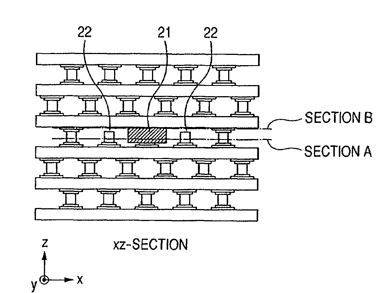
[0029]FIGS. 6A, 6B and 6C show a resonator structure D including three point defects, which is used for a resonator. The resonator structure includes two point defects each of which has no eigenmode. The resonator structure D in a first embodiment will be described below while comparing with a resonator structure B and a resonator structure C, each of which is composed of a point defect.
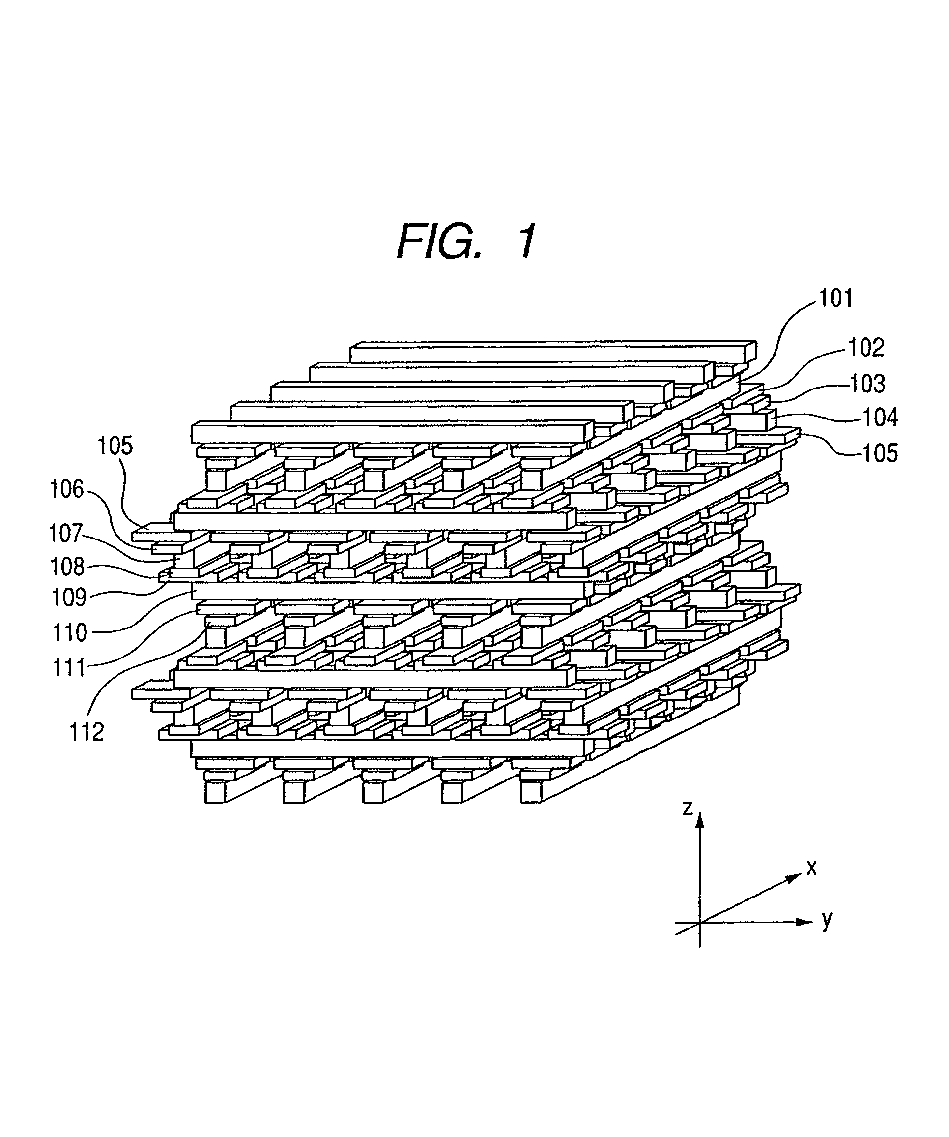
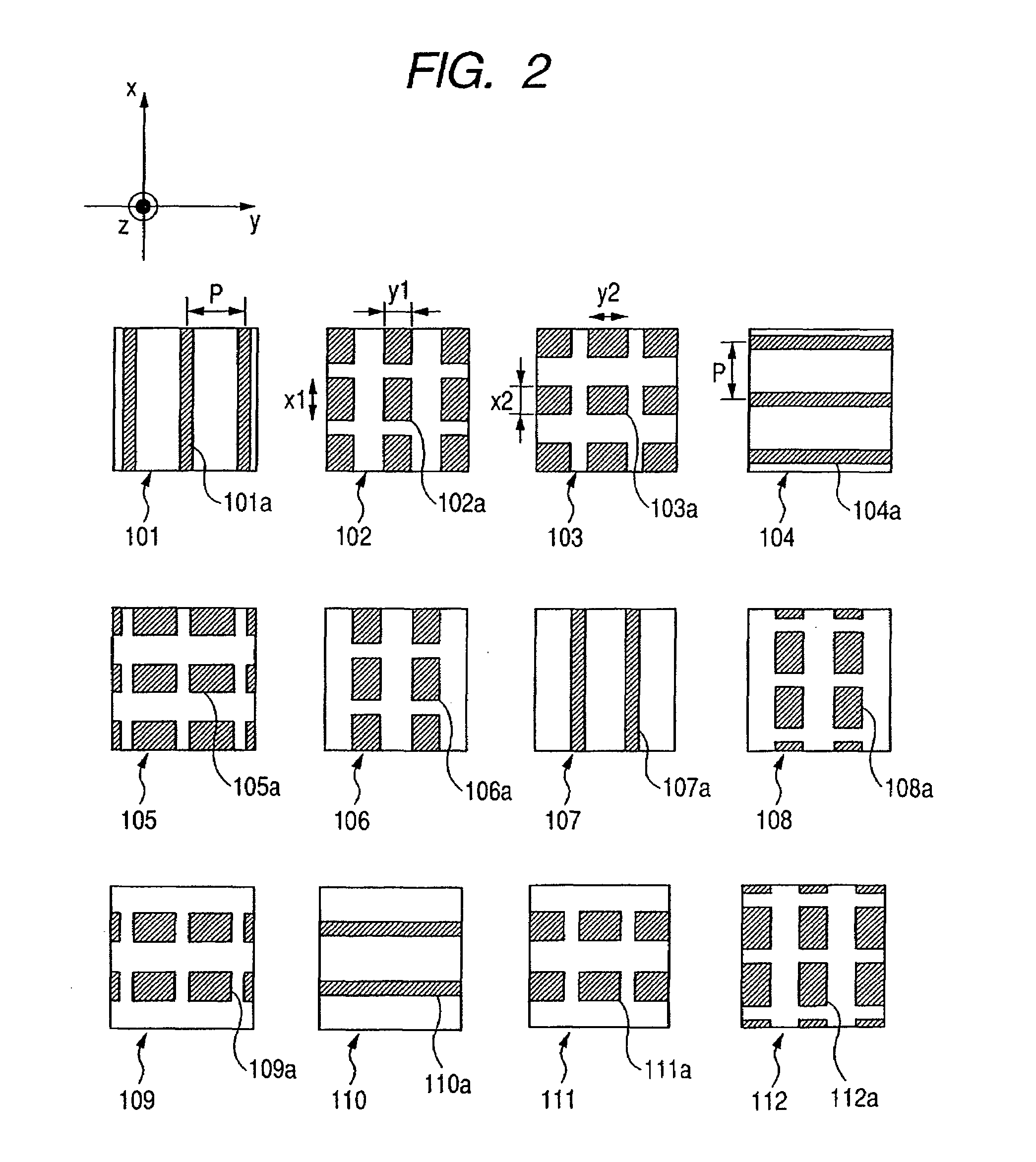
[0030]FIG. 1 is a schematic view showing a three-dimensional photonic crystal structure A having a photonic band gap wider than that of a three-dimensional photonic crystal including, for example, a conventional woodpile structure. The three-dimensional photonic crystal structure “A” includes twelve layers 101 to 112, each of which has an xy-plane, which are provided as a fundamental periodical group. FIG. 2 shows a part of an xy-section of the respective of the layers. The first (seventh) layer 101 (107) includes a plurality of columnar structures 101a (107a) which extend in an x-a...
second embodiment
(Second Embodiment)
[0055]In this embodiment, a resonator structure (structure E) in which a size of the point defect having no eigenmode is adjusted will be described.
[0056]FIGS. 8A and 8B are schematic views showing the structure E. The structure E includes a defect structure E′1 and defect structures E′2 and E′3. Each of the defect structures E′2 and E′3 has no eigenmode. Table 6 shows the specific details of the structure E. Table 7 shows normalized frequencies of the resonance modes in the structure E.
[0057]
TABLE 6Structure EPhotonic Crystal StructureRefractive Index2.4In-plane Lattice PeriodPOut-of-plane Lattice Period1.4PRod Width0.30PRod Height0.25PDiscrete Structure Width Ex10.60PDiscrete Structure Width Ey10.40PDiscrete Structure Height Ez10.05PDiscrete Structure Width Ex20.40PDiscrete Structure Width Ey20.60PDiscrete Structure Height Ez20.05PPoint Defect StructureDefect Structure E′1Center Coordinates (x, y, z)(0.00P, 0.00P, 0.00P)Refractive Index2.4Defect Structure Width ...
third embodiment
(Third Embodiment)
[0060]In this embodiment, a resonator structure (structure F) in which the number of point defects is changed or an arrangement of the point defects is changed will be described.
[0061]FIGS. 9A and 9B are schematic views showing the structure F. The structure F includes a defect structure F′1 and defect structures F′2 to F′9. Each of the defect structures F′2 to F′9 has no eigenmode. Table 8 shows the specific details of the structure F. Table 9 shows normalized frequencies of the resonance modes in the structure F.
[0062]
TABLE 8Structure FPhotonic Crystal StructureRefractive Index2.4In-plane Lattice PeriodPOut-of-plane Lattice Period1.4PRod Width0.30PRod Height0.25PDiscrete Structure Width Fx10.60PDiscrete Structure Width Fy10.40PDiscrete Structure Height Fz10.05PDiscrete Structure Width Fx20.40PDiscrete Structure Width Fy20.60PDiscrete Structure Height Fz20.05PPoint Defect StructureDefect Structure F′1Center Coordinates (x, y, z)(0.00P, 0.00P, 0.00P)Refractive Inde...
PUM
 Abstract
Description
Claims
Application Information