Integrated lens system for image sensor and method for manufacturing the same

a technology of image sensor and integrated lens, which is applied in the field of semiconductor devices, can solve the problems of high cost, difficult to maintain the desired small focus shift while using plastic lenses, and high cost of known methods of producing glass lenses, and achieve the effect of low cos

Active Publication Date: 2007-05-08
APTINA IMAGING CORP
View PDF3 Cites 113 Cited by
  • Summary
  • Abstract
  • Description
  • Claims
  • Application Information

AI Technical Summary

Benefits of technology

[0007]Exemplary embodiments of the invention provide a lens system including a first substantially hemispherical lens, a second spherical lens, and a third substantially hemispherical lens. The lenses are held together by a bonding material such as epoxy, which may also include a light absorbing dye. The invention also relates to a low-cost method of manufacturing the lens system using glass.

Problems solved by technology

Plastic lenses and mounts, typically used in current lens assemblies, show a strong variation of indices of refraction and mechanical dimensions depending upon the temperature, therefore the desired small focus shift is difficult to maintain while using plastic lenses.
Glass lenses provide a much higher level of stability, but the cost is also much higher.
The high cost of known methods of producing glass lenses can be prohibitive for implementing glass lenses in mobile image sensors.

Method used


Image

  • Integrated lens system for image sensor and method for manufacturing the same
  • Integrated lens system for image sensor and method for manufacturing the same
  • Integrated lens system for image sensor and method for manufacturing the same

Examples


Embodiment Construction

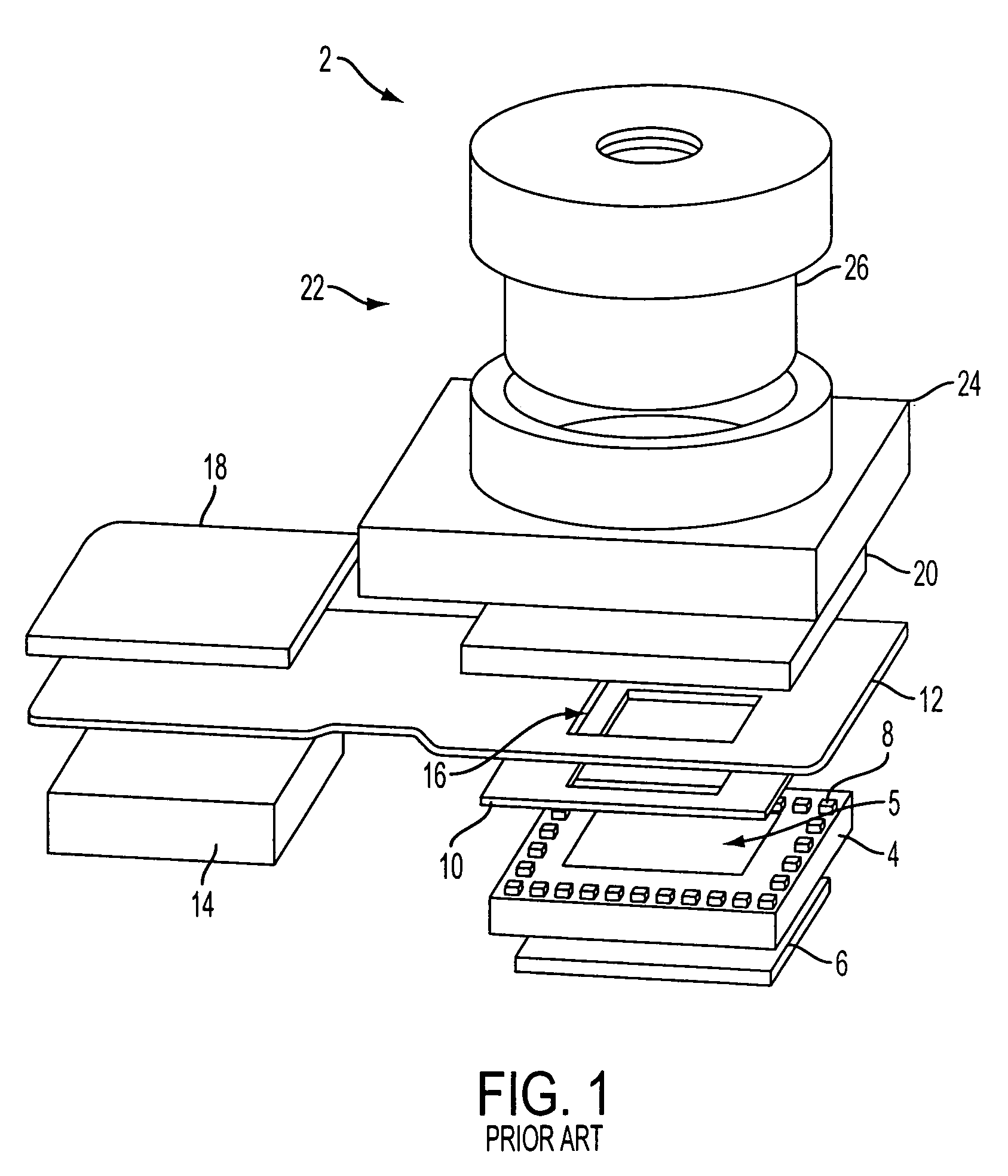
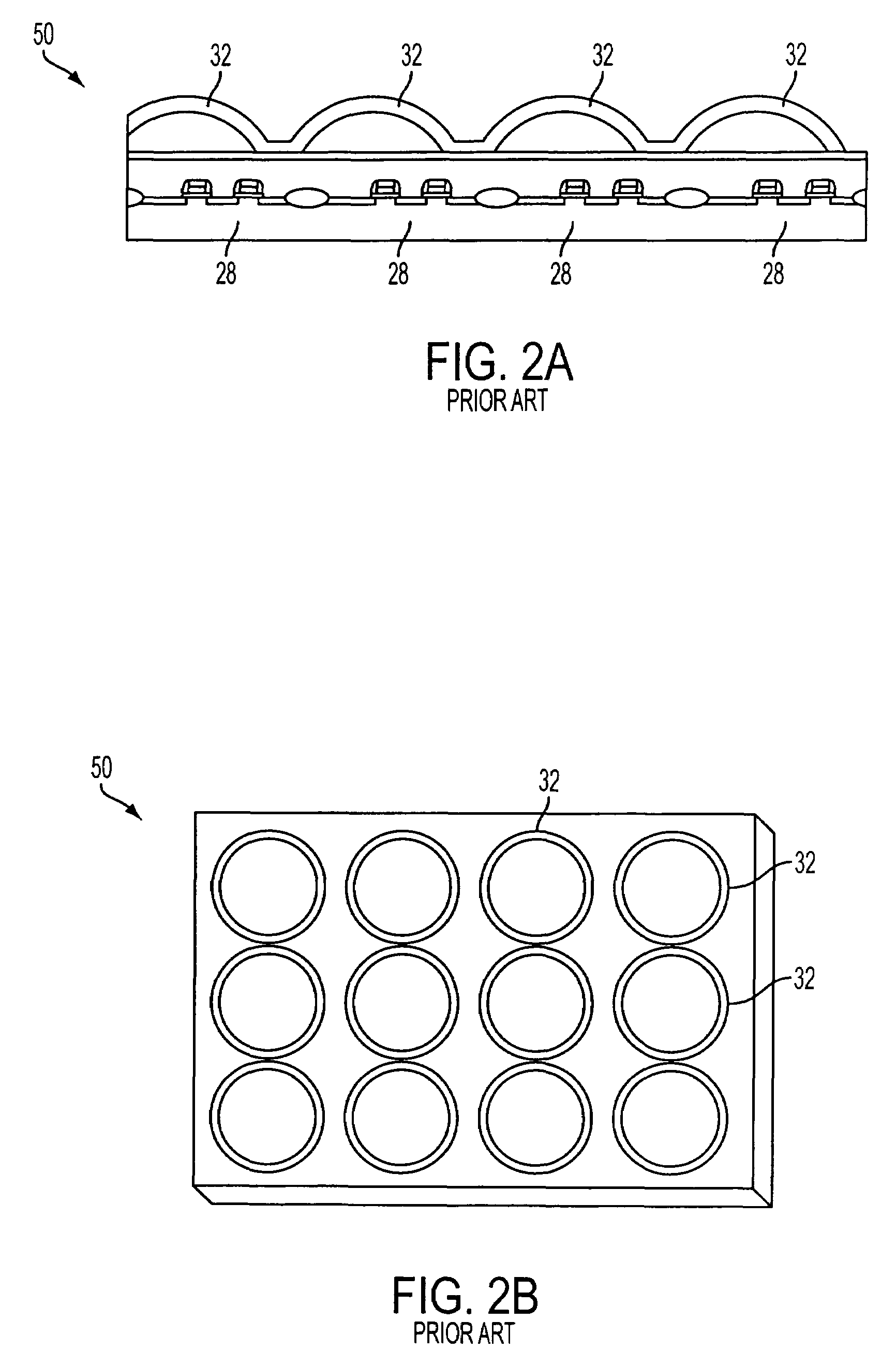
[0020]In the following detailed description, reference is made to the accompanying drawings, which form a part hereof and show by way of illustration specific embodiments in which the invention may be practiced. These embodiments are described in sufficient detail to enable those skilled in the art to practice the invention, and it is to be understood that other embodiments may be utilized, and that changes may be made without departing from the spirit and scope of the present invention. The progression of processing steps described is exemplary of embodiments of the invention; however, the sequence of steps is not limited to that set forth herein and may be changed as is known in the art, with the exception of steps necessarily occurring in a certain order.

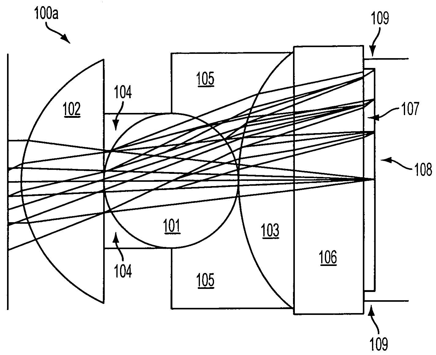
[0021]The present invention relates to a glass lens system for an imager and a low-cost manufacturing method for the lens system. Multi-element glass lens systems are an ideal solution for digital imagers. Glass lenses maintain b...


PUM


Abstract

A lens system including a first substantially hemispherical lens, a second spherical lens and a third substantially hemispherical lens. The lenses are held together by a bonding material such as epoxy, which may also include a light absorbing dye. The invention also relates to a low-cost method of manufacturing the lens system out of glass, using low cost glass ball lenses to create the hemispherical lenses.

Description

FIELD OF THE INVENTION[0001]The present invention relates to the field of semiconductor devices and, in particular, to an integrated lens system for image sensors.BACKGROUND OF THE INVENTION[0002]Integrated circuits including a semiconductor die, such as charge-coupled-devices (CCD) and complementary metal oxide semiconductor (CMOS) sensors, have commonly been used in photo-imaging applications. Such sensors typically contain thousands or millions of pixel cells in a pixel array on a single chip. Pixel cells convert light into an electrical signal that can then be stored and recalled by an electrical device such as, for example, a processor.[0003]Semiconductor dies typically are packaged and inserted into imaging devices such as, for example, digital cameras. FIG. 1 illustrates a conventional image sensor module 2, shown in an exploded perspective view. Module 2 includes a semiconductor die 4 disposed on a cushion 6 and having series of bump pad connectors 8 located adjacent the fou...

Claims


Application Information

Patent Timeline
Patent Type & Authority Patents(United States)
IPC IPC(8): G02B3/00G02B7/02H04N5/369
CPCG02B3/0056G02B7/027G02B13/005G02B1/00
Inventor BAKIN, DMITRY
Owner APTINA IMAGING CORP
Why Eureka
Try Eureka