Method for processing a substrate, method for manufacturing a semiconductor chip, and method for manufacturing a semiconductor chip having a resin adhesive layer

Active Publication Date: 2011-01-20
PANASONIC CORP
View PDF6 Cites 81 Cited by
  • Summary
  • Abstract
  • Description
  • Claims
  • Application Information

AI Technical Summary

Benefits of technology

[0013]The above-described method for manufacturing a semiconductor chip by cutting a semiconductor wafer into semiconductor chips each having a resin adhesive layer and including semiconductor apparatuses by plasma etching proceeds as follows. First, a liquid-repellent pattern is formed by printing a liquid-repellent liquid on the scribe lines on the rear surface opposite to the circuit-forming face of the semiconductor wafer, the scribe lines being the boundaries between the semiconductor chips. Next, a resin film thicker than the liquid-repellen

Problems solved by technology

In recent years, semiconductor chips are decreasing in thickness, and therefore, becoming harder to handle.
However, these conventional mask forming processes are costly.
More specifically, the mask formation based on photolithography is high cost because photolithography is intended to be used for the formation of high precision patterns of inte

Method used


Image

  • Method for processing a substrate, method for manufacturing a semiconductor chip, and method for manufacturing a semiconductor chip having a resin adhesive layer
  • Method for processing a substrate, method for manufacturing a semiconductor chip, and method for manufacturing a semiconductor chip having a resin adhesive layer
  • Method for processing a substrate, method for manufacturing a semiconductor chip, and method for manufacturing a semiconductor chip having a resin adhesive layer

Examples


first exemplary embodiment

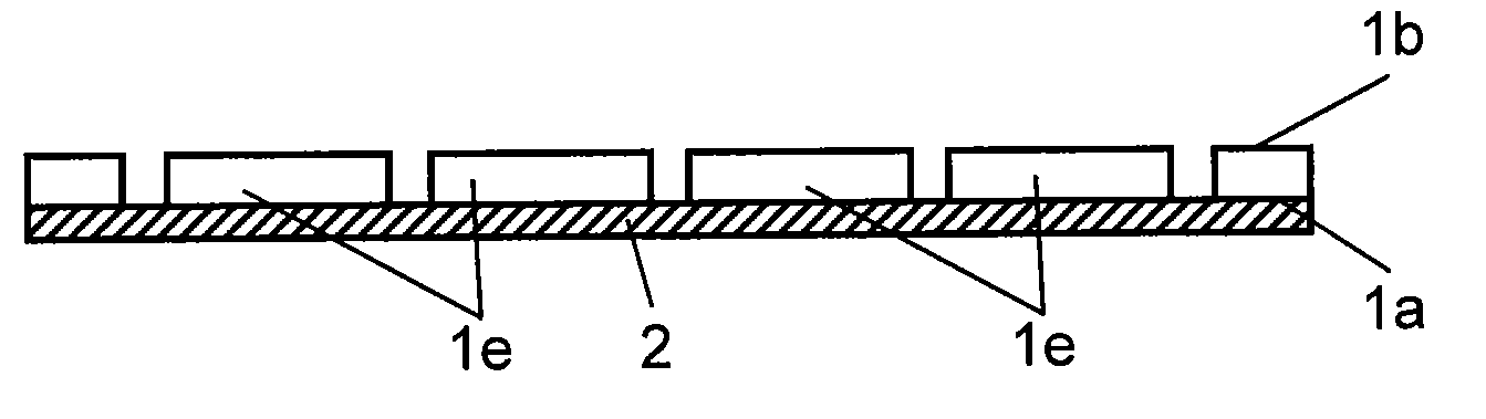
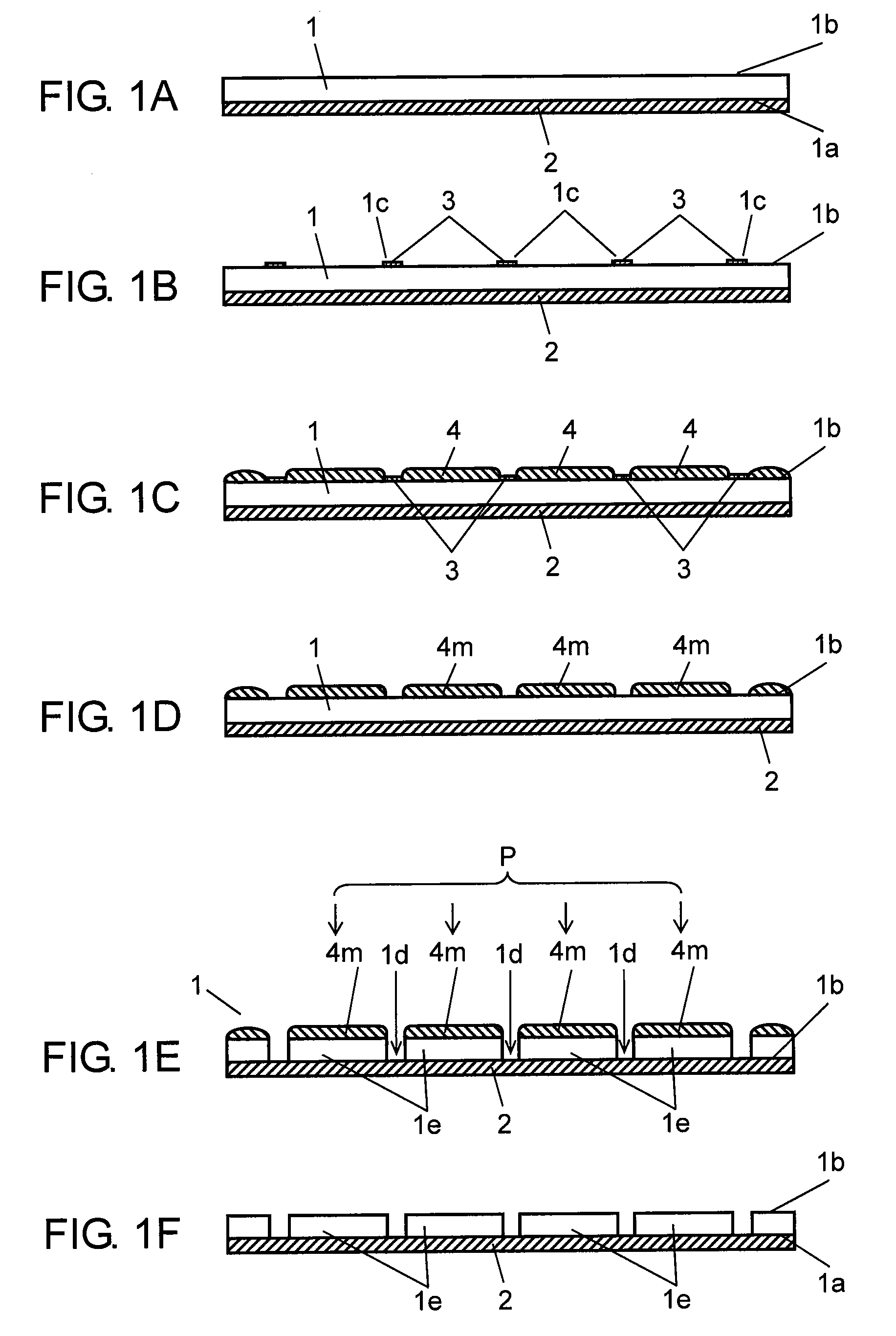
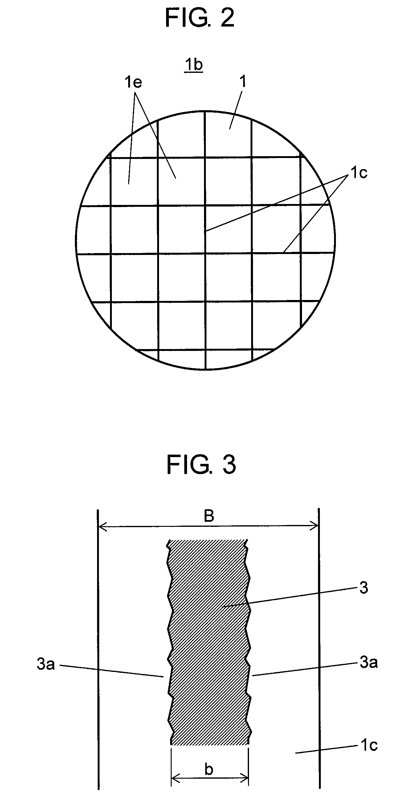
[0049]FIGS. 1A to 1F show steps of a method for processing a substrate according to a first exemplary embodiment of the present invention. FIG. 2 is a plan view of a semiconductor wafer to be processed in the method. FIG. 3 is an enlarged view of a liquid-repellent pattern used in the method. FIG. 4 is an enlarged sectional view of the semiconductor wafer to be processed in the method. FIG. 5 is an enlarged view of a liquid resin and the liquid-repellent pattern used in the method. FIG. 6 is a sectional view of a resin layer and a mask used in the method.

[0050]First, the liquid-repellent pattern and the mask used in the present exemplary embodiment will be described as follows. The liquid-repellent pattern is a resin (a repellent agent) which repels a solvent in a liquid resin that will become the mask as described later. This pattern can be formed by printing a liquid containing a repellent agent dissolved in a solvent (a liquid-repellent liquid) in a predetermined pattern and then...

second exemplary embodiment

[0066]FIGS. 7A to 7F show steps of a method for manufacturing a semiconductor chip having a resin adhesive layer according to a second exemplary embodiment of the present invention. FIG. 8 is an enlarged view of a liquid-repellent pattern used in the method. FIG. 9 is an enlarged sectional view of a semiconductor wafer to be plasma diced in the method. FIGS. 10A to 10D show steps of bonding a semiconductor chip having a resin adhesive layer manufactured in the method.

[0067]The present second exemplary embodiment shows a method for manufacturing a semiconductor chip by applying the method for processing a substrate shown in the first exemplary embodiment. In the second exemplary embodiment, the resin film used as the mask for plasma etching in the first exemplary embodiment is used as a resin adhesive layer for die bonding. In FIGS. 7A to 9, like components are labeled with like reference numerals with respect to the first exemplary embodiment.

[0068]The liquid-repellent pattern to be...


PUM


Abstract

A mask used when a semiconductor wafer is diced into individual semiconductor chips by plasma etching is formed as follows. First, a pattern of a liquid-repellent film is formed by printing a liquid-repellent liquid on the area to be etched on the rear surface of the semiconductor wafer. Next, a resin film thicker than the liquid-repellent film is formed in the area not having the liquid-repellent film by supplying a liquid resin to the rear surface on which the liquid-repellent pattern has been formed. Then, the resin film is cured to form the mask covering the area other than the area to be removed by the etching. This method allows the formation of an etching mask without using a high-cost method such as photolithography.

Description

TECHNICAL FIELD[0001]The present invention relates to a method for processing a substrate such as a semiconductor wafer so as to partially remove it, a method for manufacturing a semiconductor chip by applying the method for processing a substrate, and a method for manufacturing a semiconductor chip having a resin adhesive layer.BACKGROUND ART[0002]Semiconductor devices mounted on an electronic device substrate or the like are manufactured by cutting a semiconductor wafer into semiconductor chips each including individual semiconductor apparatuses as integrated circuits implemented in a wafer state. In recent years, semiconductor chips are decreasing in thickness, and therefore, becoming harder to handle. In line with this, it has been proposed to cut a semiconductor wafer into semiconductor chips by plasma etching, which is called plasma dicing.[0003]Plasma dicing means to cut a semiconductor wafer along lattice-shaped scribe lines indicating cutting positions by plasma etching, wh...

Claims


Application Information

Patent Timeline
IPC IPC(8): H01L21/3065
CPCH01L21/0273H01L21/78H01L21/3086H01L2224/83191
Inventor HAJI, HIROSHIARITA, KIYOSHI
Owner PANASONIC CORP
Why Eureka
Try Eureka