System for processing a workpiece

a workpiece and workpiece technology, applied in the direction of chemistry apparatus and processes, cleaning using liquids, coatings, etc., can solve the problems of microelectronic end product defects or failures, time, labor and effort required to manufacture microelectronic devices, and reduce the total amount of raw materials, process fluids, etc., to reduce particle contamination, improve manufacturing microelectronic, and reduce the effect of end product defects

Inactive Publication Date: 2007-05-15
APPLIED MATERIALS INC
View PDF99 Cites 11 Cited by
  • Summary
  • Abstract
  • Description
  • Claims
  • Application Information

AI Technical Summary

Benefits of technology

[0006]A new wafer processing system has been invented that provides significant improvements in manufacturing microelectronic and similar devices. The new system reduces particle contamination. As a result there are fewer defects in the end products. This reduces the total amount of raw materials, process fluids, time, labor and effort required to manufacture microelectronic devices. Accordingly, the new wafer processing system of the present invention significantly increases manufacturing yields.
[0007]A unique workpiece processor design has been invented that significantly reduces cross contamination of process fluids. The unique design also greatly increases the ability to exhaust vapor or fumes and drain process fluids from the process chamber during processing of a semiconductor wafer. Further, the processor of the present invention utilizes a relatively simple, magnetic rotor engagement mechanism that reduces variability of vibration affects caused by variations in manufacturing techniques from one processor to another. As a result of these design improvements, the effects of wafer processing is more consistent from one workpiece processor to the next, and high manufacturing quality standards and increased efficiencies are achieved.
[0008]In one embodiment, the wafer processing system of the present invention provides a plurality of workpiece stations for plating, etching, cleaning, passivating, depositing and / or removing films and masking materials from a workpiece surface. The system includes a robot, which is moveable between the workpiece stations and moves the workpiece from one station to another. At least one of the workpiece stations includes a workpiece processor having an upper rotor and a lower rotor engageable to form a workpiece process chamber. A magnetic force between repulsing magnets is utilized to maintain contact between the rotors during operation of the processor. This unique process chamber design reduces vibrations, which have been found to be a major contributor to particulate contamination, and also reduces the chances of process fluids leaking onto the surface of processed wafers, which can result in defects or failure of the microelectronic end products.
[0009]The wafer processing system of the present invention has also been designed to increase air flow through the workpiece processor during processing. Better air flow management reduces particle contamination and increases overall processing efficiency. As a result, less time, materials and energy is consumed. Particularly, the processor of the present invention has air flow passageways in the process head, which draws ambient air from the mini-environment surrounding the processor, into the process head, and out through the bottom of the processor. Further, annular channels formed in the base and the upper rim of the base relieve pressure build up in the process chamber. During operation, openings in the upper rim of the base receive “blow-by” fluids. The annular channels bleed the “blow-by” fluids off to an exhaust port, relieving pressure build up. Moreover, an air aspirator is connected to an annulus positioned below the motor in the process head. The aspirator sucks any gaseous fluids that may come from the air flow passageways in the process head or the annular channels in the base. Additionally, a central opening in the process head and upper rotor, and a process fluid nozzle in the base which extends upwardly through an opening in the lower rotor and is connected to a snorkel permits air to be drawn directly into the workpiece processor during operation. As a result of these design improvements, air flow in the process chamber is greatly enhanced, and more uniform processing and increased efficiencies are achieved.

Problems solved by technology

This reduces the total amount of raw materials, process fluids, time, labor and effort required to manufacture microelectronic devices.
This unique process chamber design reduces vibrations, which have been found to be a major contributor to particulate contamination, and also reduces the chances of process fluids leaking onto the surface of processed wafers, which can result in defects or failure of the microelectronic end products.

Method used


Image

  • System for processing a workpiece
  • System for processing a workpiece
  • System for processing a workpiece

Examples


Embodiment Construction

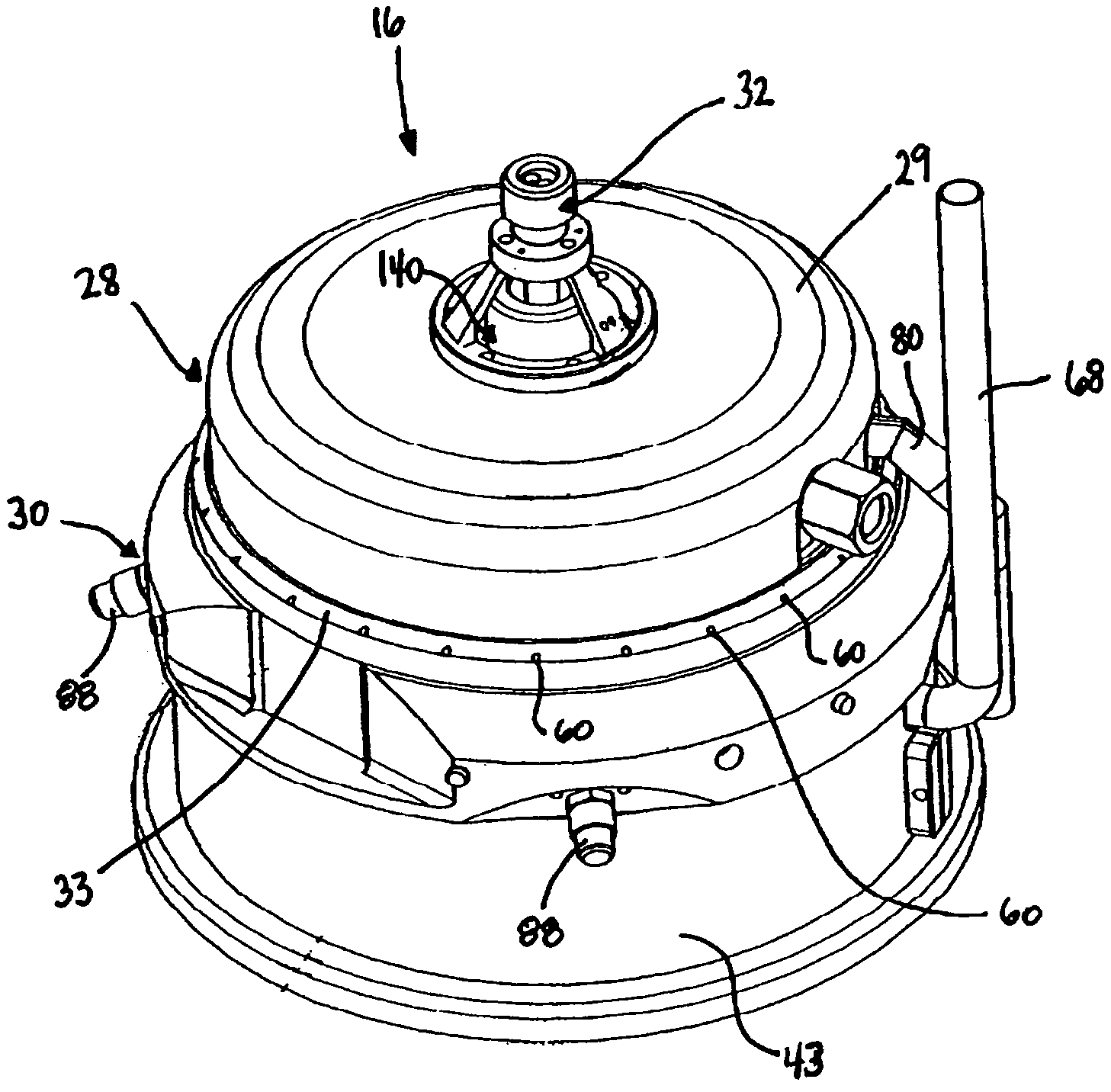
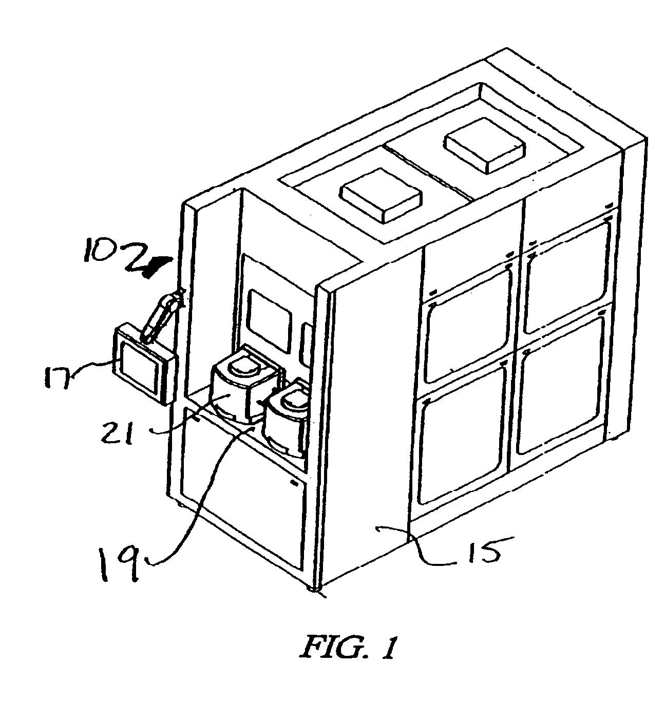
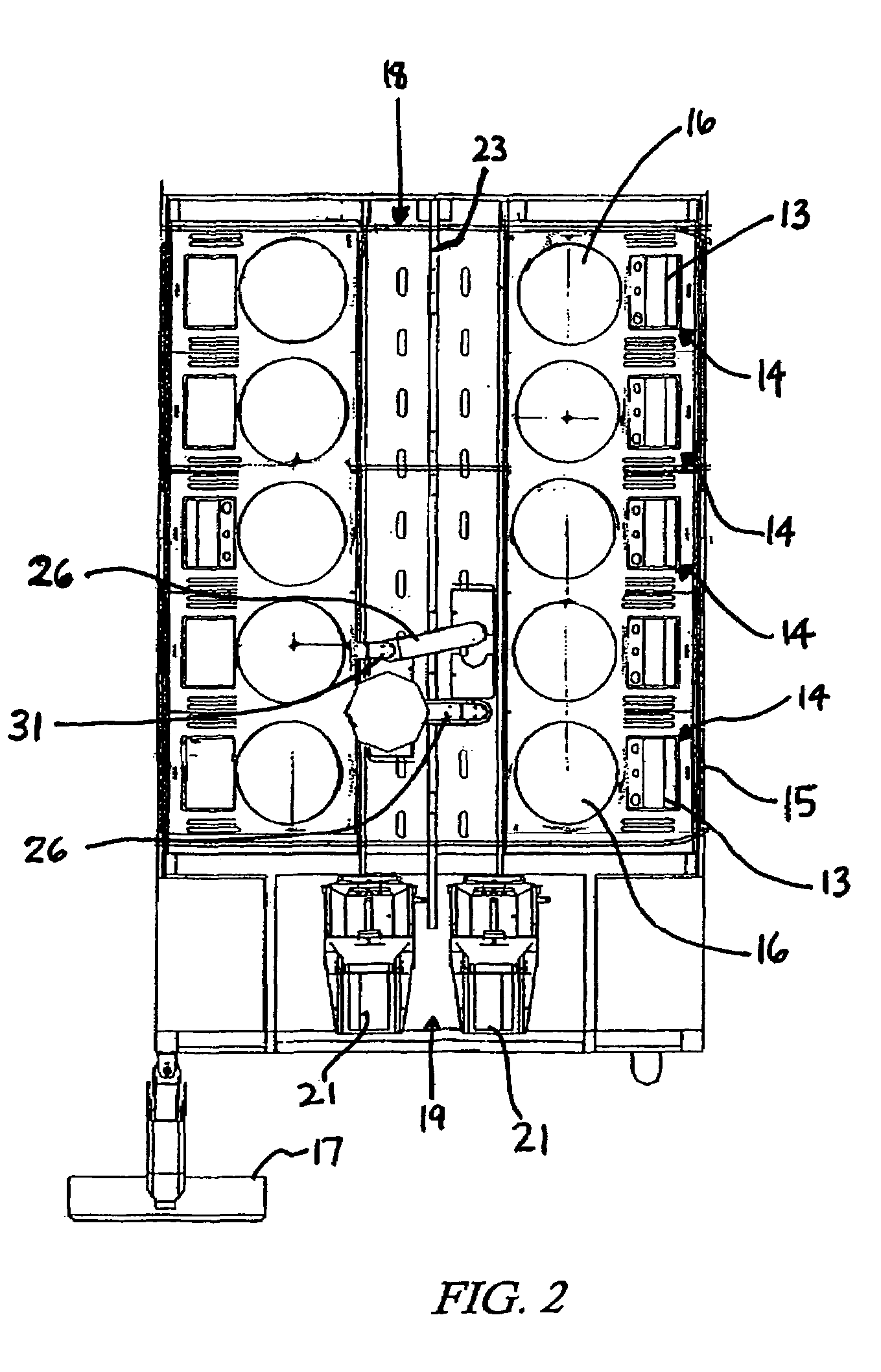
[0043]As shown in FIGS. 1–3, a processing system 10 has an enclosure 15, a control / display 17, and an input / output station 19 and a plurality of processing stations 14. Workpieces 24 are removed from carriers 21 at the input / output station 19 and processed within the system 10.

[0044]The processing system 10 includes a support structure for a plurality of processing stations 14 within the enclosure 15. At least one processing station 14 includes a workpiece processor 16 and an actuator 13 for opening and closing processor 16. The processor 16 of the present invention is designed to be utilized in a processing system 10, for example, as disclosed in pending U.S. Patent Application Ser. No. 60 / 476,786, filed Jun. 6, 2003, and U.S. Pat. Nos. 6,900,132 and 6,930,046.

[0045]These U.S. patents and application are incorporated herein by reference. System 10 may include only a plurality of processors 16 or it may include other processing modules, in addition to one or more processors 16, such...


PUM

PropertyMeasurementUnit
forceaaaaaaaaaa
magnetic forceaaaaaaaaaa
polarityaaaaaaaaaa

Abstract

A system for processing a workpiece includes a process head assembly and a base assembly. The process head assembly has a process head and an upper rotor. The base assembly has a base and a lower rotor. The base and lower rotor have magnets wherein the upper rotor is engageable with the lower rotor via a magnetic force created by the magnets. The engaged upper and lower rotors form a process chamber where a semiconductor wafer is positioned for processing. Process fluids for treating the workpiece are introduced into the process chamber, optionally while the processing head spins the workpiece. Additionally, air flow around and through the process chamber is managed to reduce particle adders on the workpiece.

Description

CROSS-REFERENCE TO RELATED APPLICATIONS[0001]This Application is a Continuation-In-Part of U.S. patent application Ser. No. 10 / 690,864, filed Oct. 21, 2003 and now U.S. Pat. No. 6,930,046, which is a Continuation-In-Part of U.S. patent application Ser. No. 10 / 202,074, filed Jul. 23, 2002 and now U.S. Pat. No. 6,794,291, which is a Continuation of U.S. patent application Ser. No. 09 / 437,711, filed Nov. 10, 1999, now U.S. Pat. No. 6,423,642, which is a Continuation-In-Part and U.S. National Phase of International Patent Application No. PCT / US99 / 05676, filed Mar. 15, 1999, published in English and designating the United States, and claiming priority to U.S. Patent Application No. 60 / 116,750, filed Jan. 22, 1999. Priority to these applications is claimed under 35 U.S.C. §§ 119, 120 and / or 365. The above-identified Applications are also incorporated herein by reference.TECHNICAL FIELD[0002]The invention relates to surface preparation, cleaning, rinsing and drying of workpieces, such as s...

Claims


Application Information

Patent Timeline
Patent Type & Authority Patents(United States)
IPC IPC(8): B05C11/02H01L21/00H01L21/3213
CPCH01L21/32134H01L21/67017H01L21/67028H01L21/6715H01L21/67173H01L21/6719H01L21/68785
Inventor HANSON, KYLE M.
Owner APPLIED MATERIALS INC
Why Eureka
Try Eureka