Bulk acoustic wave resonator and manufacturing method thereof, filter using the same, semiconductor integrated circuit device using the same, and high frequency module using the same

a technology of acoustic waves and resonators, applied in piezoelectric/electrostrictive/magnetostrictive devices, piezoelectric/electrostriction/magnetostriction machines, electrical apparatus, etc., can solve the problem of difficult to obtain excellent resonance characteristics production costs increase, and the frequency accuracy of bulk acoustic wave resonators and bulk acoustic wav

Inactive Publication Date: 2007-05-22
HITACHI MEDIA ELECTORONICS CO LTD
View PDF9 Cites 22 Cited by
  • Summary
  • Abstract
  • Description
  • Claims
  • Application Information

AI Technical Summary

Benefits of technology

[0016]In the conventional art disclosed in the patent document 1, the orientation of the piezoelectric layer is deteriorated due to affect by the surface condition of the sacrificial layer so that it is difficult to obtain an excellent resonance characteristic in the bulk acoustic wave resonator. In the conventional art disclosed in the patent document 2, the number of the process to form the bulk acoustic wave resonator is increased so that the production cost is increased.
[0024]According to the present invention, the bulk acoustic wave resonator and the bulk acoustic wave resonator filter can be downsized. Additionally according to the present invention, the frequency accuracy of the bulk acoustic wave resonator and the bulk acoustic wave resonator filter can be improved so that the yield is increased.

Problems solved by technology

However, the present inventors found the following problems as the result of the consideration of the above mentioned conventional art.
Therefore, the opening area of the cavity on the rear face of the substrate is enlarged so that it is not appropriate to downsize the bulk acoustic wave resonator.
In the conventional art disclosed in the patent document 1, the orientation of the piezoelectric layer is deteriorated due to affect by the surface condition of the sacrificial layer so that it is difficult to obtain an excellent resonance characteristic in the bulk acoustic wave resonator.
In the conventional art disclosed in the patent document 2, the number of the process to form the bulk acoustic wave resonator is increased so that the production cost is increased.

Method used


Image

  • Bulk acoustic wave resonator and manufacturing method thereof, filter using the same, semiconductor integrated circuit device using the same, and high frequency module using the same
  • Bulk acoustic wave resonator and manufacturing method thereof, filter using the same, semiconductor integrated circuit device using the same, and high frequency module using the same
  • Bulk acoustic wave resonator and manufacturing method thereof, filter using the same, semiconductor integrated circuit device using the same, and high frequency module using the same

Examples


embodiment 1

[0038](Embodiment 1)

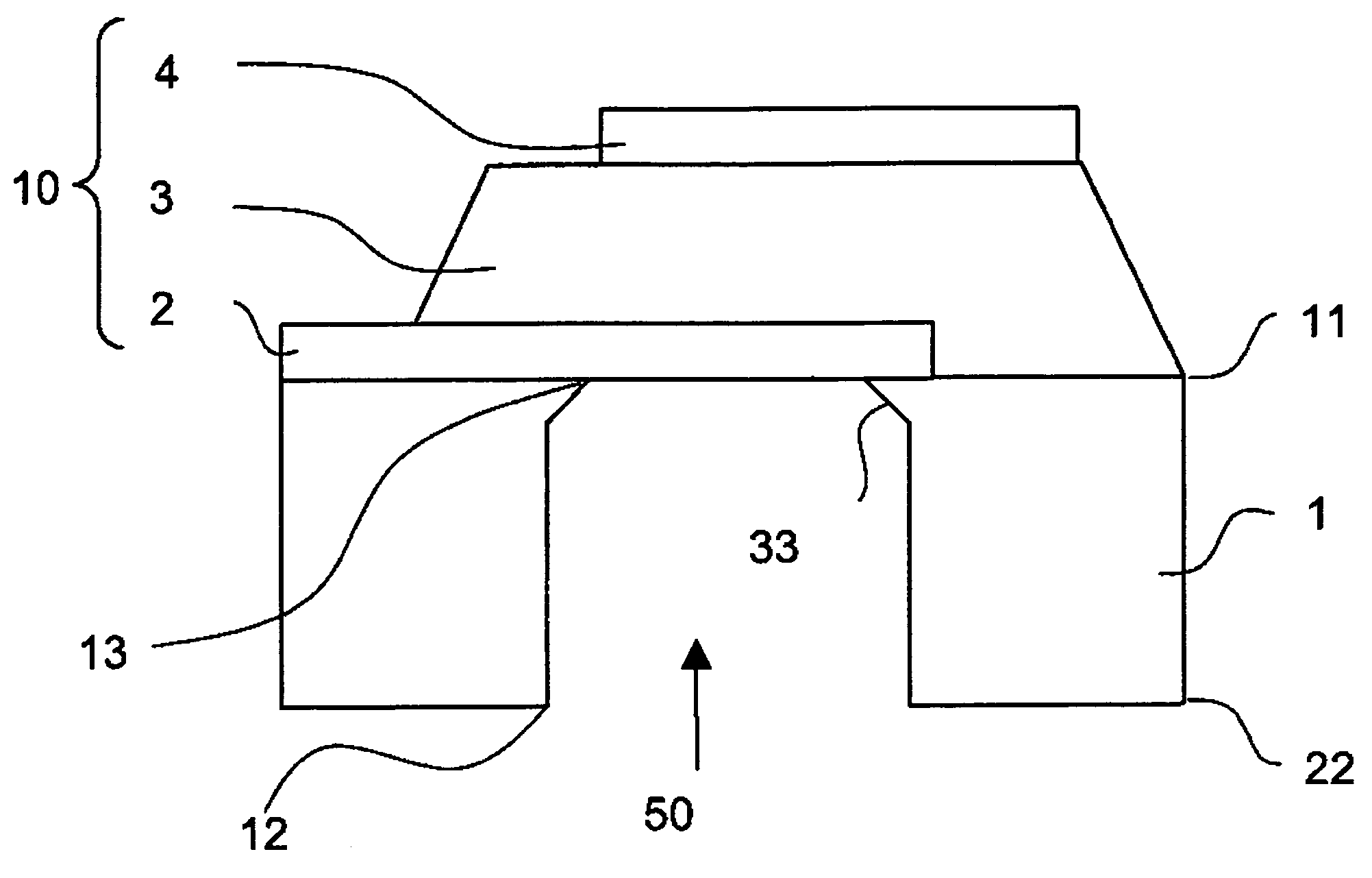
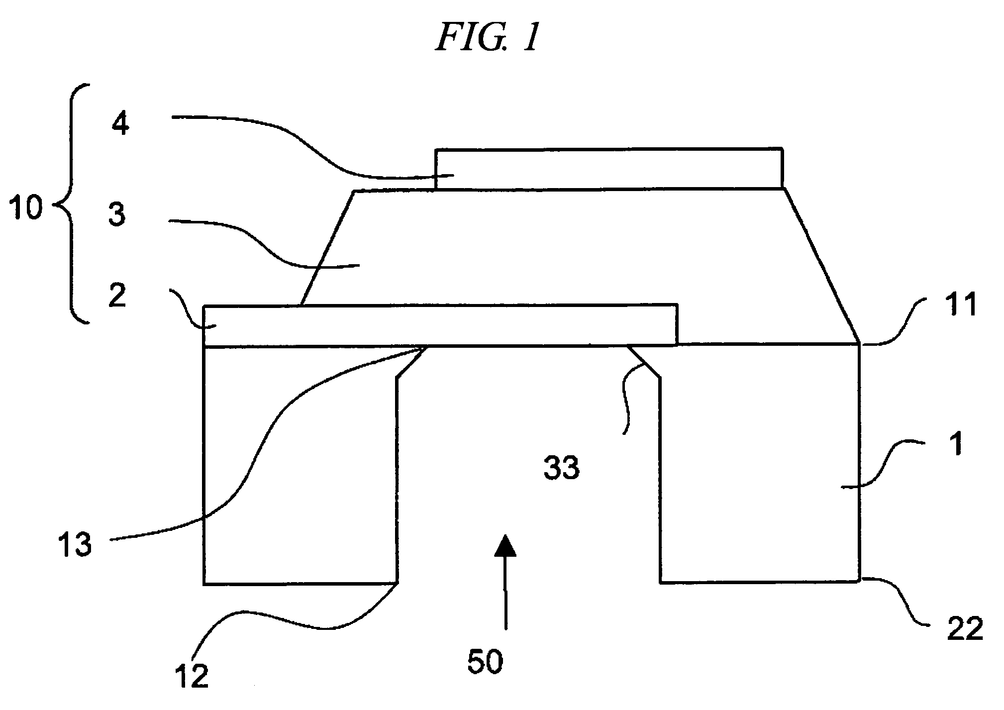
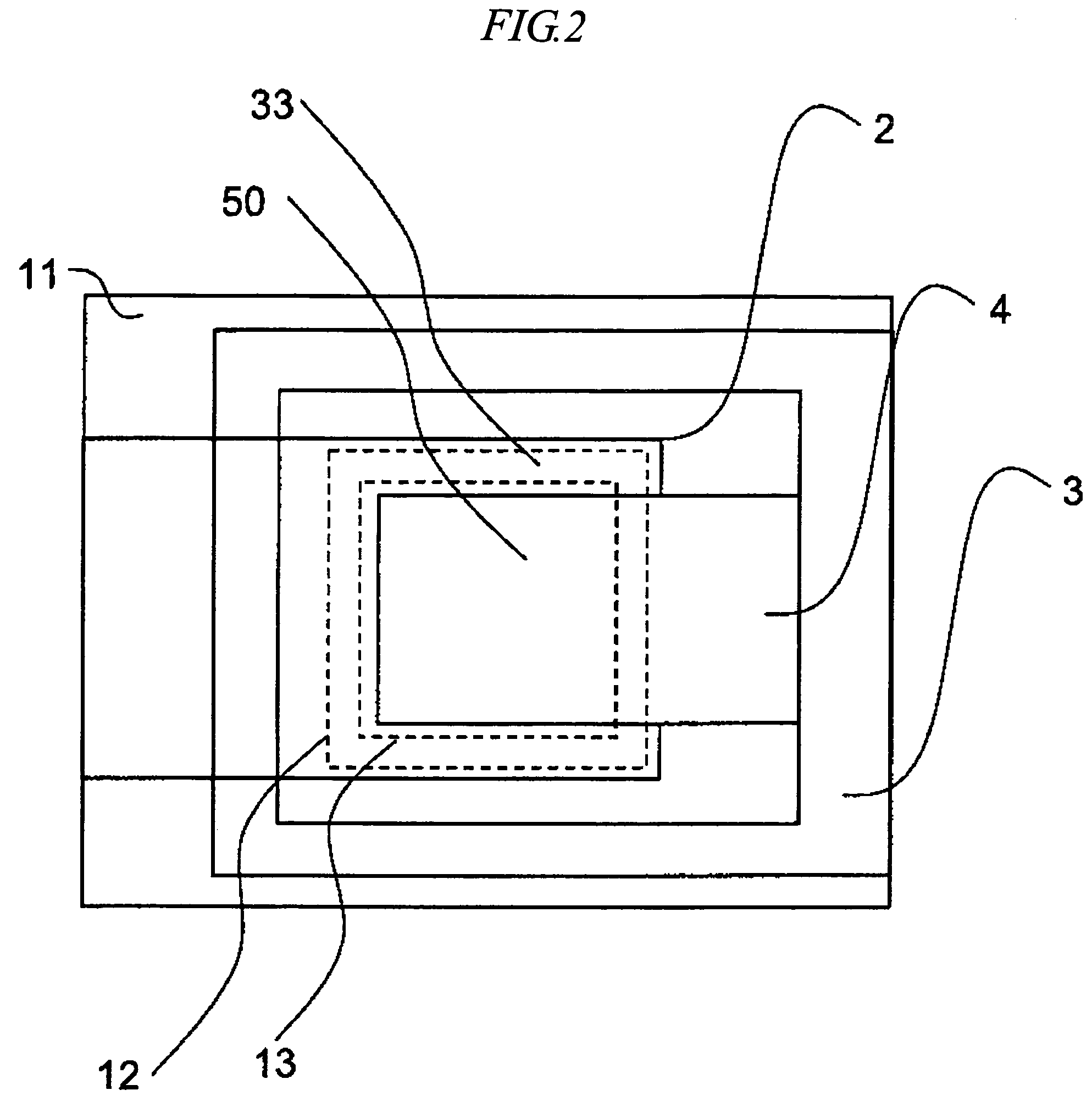
[0039]FIG. 1 is a sectional view of the embodiment 1 of the bulk acoustic wave resonator according to the present invention. A substrate 1 to form the bulk acoustic wave resonator of FIG. 1 is a single crystal Si (100) substrate having a first surface 11 equivalent to a (100) plane and a second surface 22 opposite to the first surface. A stacked resonator 10 including a first electrode layer 2 in contact with the first surface 11, a piezoelectric layer 3 overlaying the first electrode layer 2 and a second electrode layer 4 overlaying the piezoelectric layer 3 is provided on the first surface 11 of the substrate 1. An air gap 50 is formed through the substrate 1 in the area corresponding to the stacked resonator 10 on the substrate 1. The stacked resonator 10 has a diaphragm structure in which the piezoelectric layer 3 is sandwiched between the first electrode layer and the second electrode layer in the stacked direction. The first electrode layer and the second e...

embodiment 2

[0048](Embodiment 2)

[0049]FIG. 4 is a sectional view of another embodiment of the bulk acoustic wave resonator according to the present invention. The substrate 1, the first electrode layer 2, the piezoelectric layer 3 overlaying the first electrode layer 2, the second electrode layer 4 overlaying the piezoelectric layer 3 and the air gap 50 formed in the substrate 1 of FIG. 4 are same as the embodiment 1. The difference from the embodiment 1 is that an underlayer 6 in contact with the first surface 11 of the substrate 1 is provided between the substrate 1 and the first electrode layer 2. At least a portion of the underlayer 6 is positioned to overlap with the aperture of the air gap opening at the first surface 11 and having the tapered shape in the stacked direction. The underlayer 6 is exposed to the air gap 50 thereby to be acoustically isolated from the electrical signal by the air.

[0050]In the bulk acoustic wave resonator of the present embodiment, for example, the underlayer ...

embodiment 3

[0055](Embodiment 3)

[0056]Now, an embodiment that the filter using the bulk acoustic wave resonator according to the present invention is formed on the single substrate is described. FIG. 7 is a circuit diagram of the cellular phone applied the filter using the bulk acoustic wave resonator according to the present invention. The detailed configuration of the filter is described later.

[0057]In FIG. 7, a high frequency received signal Rx received from an antenna ANT is passed through a phase shifter 130 and inputted into a low noise amplifier 150 to be amplified through a receiving filter 79 to remove image frequency signals and selectively pass frequency signals in a predetermined receiving band. The high frequency received signal Rx amplified by the low noise amplifier 150 is transmitted to a baseband unit 155 to convert to baseband through a receiving mixer 153.

[0058]Meanwhile, a high frequency transmitting signal Tx transmitted from the baseband unit 155 is inputted into a power a...


PUM


Abstract

A bulk acoustic wave resonator in which the problem of the technology for forming the diaphragm structure is resolved, which is more compact and improved the frequency accuracy, and the manufacturing method thereof, a filter using the same, a semiconductor integrated circuit device using the same, and a high frequency module using the same are provided. The bulk acoustic wave resonator according to the present invention comprises a substrate having a first surface and a second surface opposite to the first surface, and a staked resonator including a first electrode film in contact with the first surface, a piezoelectric film overlaying the first electrode film and a second electrode film overlaying the piezoelectric film. The substrate is provided with an air gap including a first aperture opening at the first surface and a second aperture opening at the second surface at the position corresponding to the staked resonator, respectively and having air gap generally vertical shape to the first surface, and another air gap having a tapered shape in the vicinity of the first surface.

Description

CROSS-REFERENCE TO RELATED APPLICATION[0001]The present application claims priority from Japanese patent application No. JP 2004-372534 filed on Dec. 24, 2004, the content of which is hereby incorporated by reference into this application.FIELD OF THE INVENTION[0002]The present invention relates to a resonator using acoustic wave, especially, a bulk acoustic wave resonator using bulk acoustic wave, a filter using the same (hereinafter referred to as a bulk acoustic wave resonator filter) and a manufacturing method thereof.BACKGROUND OF THE INVENTION[0003]Along with the popularization of mobile communication as represented by cellular phones, the demand for a high frequency filter operated in several hundred MHz-several GHz has been increased. Among various filter technologies, the filter manufactured by using a bulk acoustic wave resonator is characterized by (1) high frequency, (2) compact, (3) excellent temperature characteristic, and (4) excellent electric strength.[0004]The bulk...

Claims


Application Information

Patent Timeline
Patent Type & Authority Patents(United States)
IPC IPC(8): H03H9/00H01L41/00H03H3/02H03H9/17H03H9/58
CPCH03H3/02H03H9/0542H03H9/0571H03H9/174H03H9/564H03H9/706
Inventor ASAI, KENGOMATSUMOTO, HISANORIISOBE, ATSUSHIHIKITA, MITSUTAKA
Owner HITACHI MEDIA ELECTORONICS CO LTD
Why Eureka
Try Eureka