Semiconductor device and system having semiconductor device mounted thereon

a semiconductor device and semiconductor technology, applied in the direction of printed circuit assembling, printed circuit manufacturing, printed circuit aspects, etc., can solve the problems of reduced connection pin and connection pin area of semiconductor devices, reduced and increased wiring density of wiring patterns. , to achieve the effect of facilitating routing of wiring patterns and reducing wiring density

Inactive Publication Date: 2007-05-29
SOCIONEXT INC
View PDF12 Cites 18 Cited by
  • Summary
  • Abstract
  • Description
  • Claims
  • Application Information

AI Technical Summary

Benefits of technology

[0012]The present invention has been made in view of the above circumstances, and an object thereof is to provide a semiconductor device which makes it possible to reduce wiring density of a wiring pattern on a mounting board, thereby facilitating routing of the wiring pattern.

Problems solved by technology

However, these packages are limited in their capability of coping with increase in the number of connection pins and reduction in the area of the semiconductor device.
However, the semiconductor device is further making a progress toward still higher integration of elements therein, resulting in an even larger number of connection pins provided thereon.
This increases the wiring density of a wiring pattern on a mounting board, which makes the wiring pattern difficult to be routed.

Method used


Image

  • Semiconductor device and system having semiconductor device mounted thereon
  • Semiconductor device and system having semiconductor device mounted thereon
  • Semiconductor device and system having semiconductor device mounted thereon

Examples


Embodiment Construction

[0031]The invention will now be described in detail with reference to the drawings showing a preferred embodiment thereof.

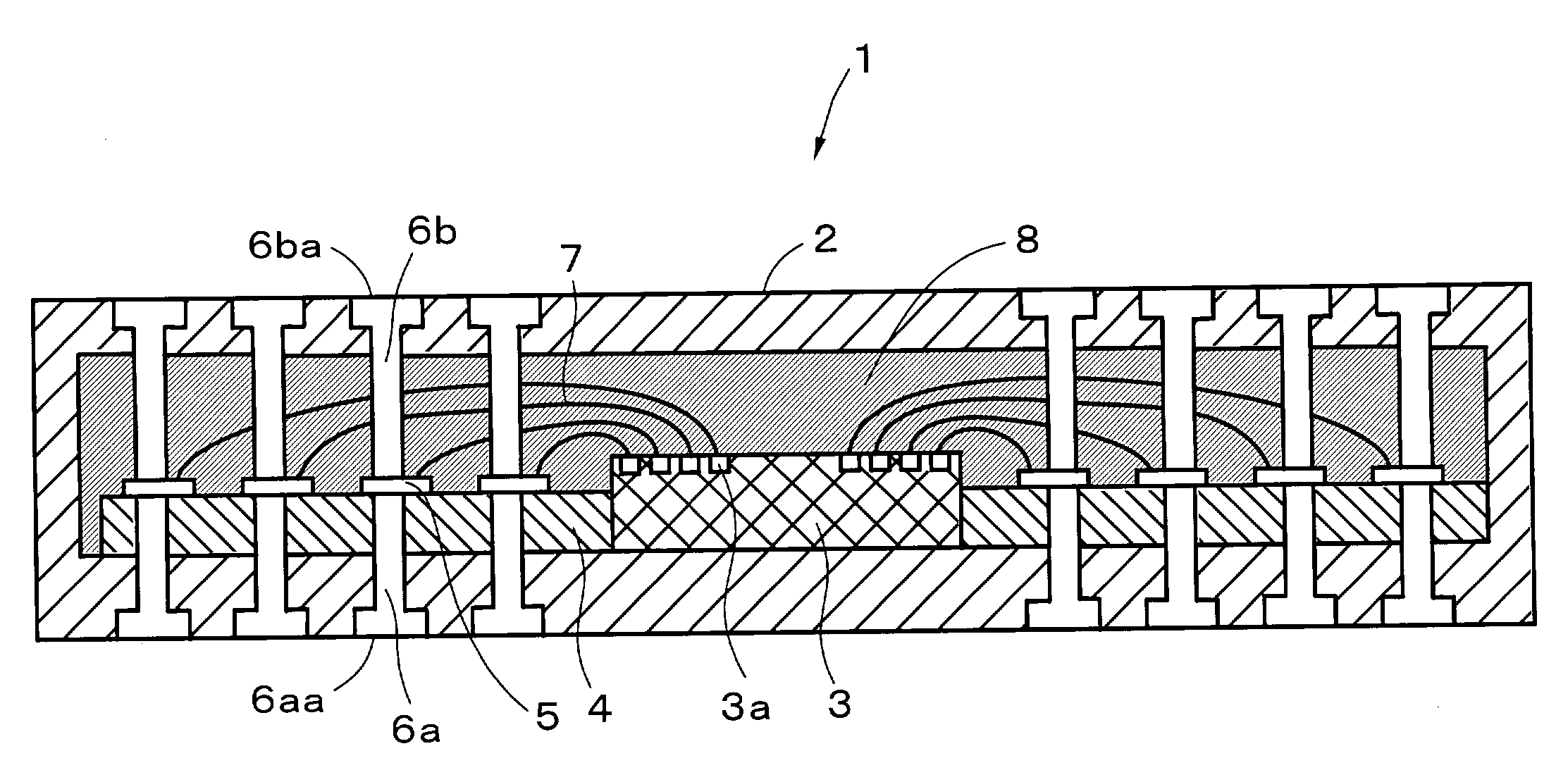
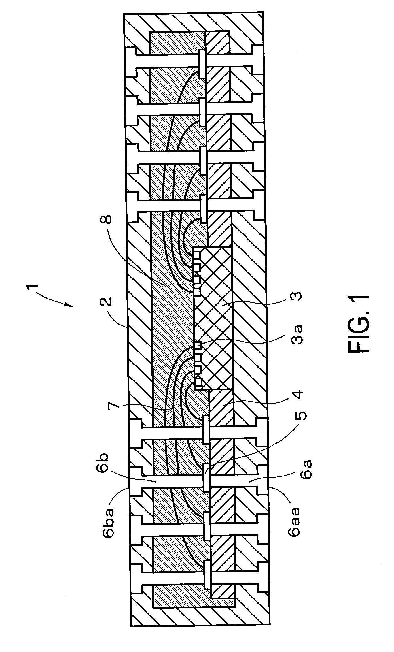
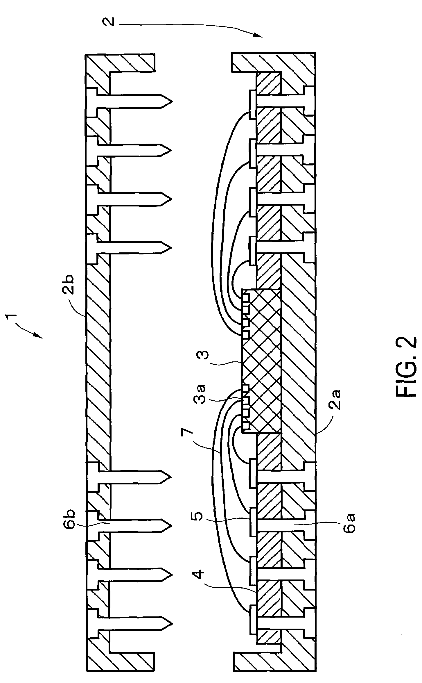
[0032]FIG. 1 is a longitudinal sectional view of a semiconductor device according to a first embodiment of the present invention. The semiconductor device shown in FIG. 1 is comprised of a package 2, a bare chip 3 fixed to a central portion of an inner bottom surface of the package 2, an inner board 4 fixed to the inner bottom surface of the package 2 in a state fitted to the periphery of the bare chip 3, pads 5 fixed to an upper surface of the inner board 4 and connected to signal lines of the bare chip 3, respectively, vias 6a extending from the respective pads 5 to an outer bottom surface of the package 2, vias 6b extending from the respective pads 5 to an outer top surface of the package 2, bonding wires 7 for connecting the bare chip 3 and the pads 5, and a mold 8 filled within the package 2.

[0033]The bare chip 3 has pads 3a formed on a top surface thereof f...


PUM


Abstract

A ball grid array packaged semiconductor device mounted on a mounting board and including pads formed within a package and are connected to signal lines of a bare chip by bonding wires. There are formed first vias extending from the respective pads to a bottom surface of a package, and second vias extending from the same respective pads to a top surface of the package to form continuous vias. This makes it possible to connect the mounting boards to the top and bottom surfaces of the package, thereby enabling reduction of the wiring density of wiring patterns on the mounting boards, and thereby facilitating routing of the wiring patterns on the mounting boards. The semiconductor device is capable of reducing wiring density of the wiring pattern on the mounting board.

Description

BACKGROUND OF THE INVENTION[0001](1) Field of the Invention[0002]This invention relates to a semiconductor device and a system having the semiconductor device mounted thereon, and more particularly to a ball grid array packaged semiconductor device and a system having the ball grid array packaged semiconductor device mounted thereon.[0003](2) Description of the Related Art[0004]These days, with the progress of higher integration of elements into semiconductor devices, each semiconductor device has an increasing number of connection pins for connection to a mounting board. Further, to reduce the area of the semiconductor device, a narrower pin pitch is employed.[0005]Packages of semiconductor devices include a QFP (Quad Flat Package), an SQFP (Shrink Quad Flat Package), and so forth. However, these packages are limited in their capability of coping with increase in the number of connection pins and reduction in the area of the semiconductor device. To overcome the problem, recently, ...

Claims


Application Information

Patent Timeline
Patent Type & Authority Patents(United States)
IPC IPC(8): H01L23/06H01L23/055H01L23/12H01L23/24H01L23/498H01L25/10H05K3/34
CPCH01L23/055H01L23/24H01L23/49816H01L25/105H05K3/3463H01L25/16H01L2224/48091H01L2224/48227H01L2924/01079H01L2924/15331H01L2924/16152H01L2924/19041H05K3/3436H05K2201/10515H05K2203/047H01L2924/00014H01L24/48H01L2225/1058H01L2224/05599H01L2224/85444H01L2924/181H01L2224/45099H01L2924/00012H01L2224/45015H01L2924/207
Inventor SHIBATA, MANABU
Owner SOCIONEXT INC
Why Eureka
Try Eureka