Wire trimmed programmable logic array

Inactive Publication Date: 2007-05-29
IBM CORP
View PDF20 Cites 6 Cited by
  • Summary
  • Abstract
  • Description
  • Claims
  • Application Information

AI Technical Summary

Benefits of technology

[0012]FIGS. 3A and 3B illustrate the interconnection by

Problems solved by technology

PLA technology does, however, tend to exhibit higher power consumption.
While the simplicity inherent in interconnection by abutment designs is desira

Method used


Image

  • Wire trimmed programmable logic array
  • Wire trimmed programmable logic array
  • Wire trimmed programmable logic array

Examples


Embodiment Construction

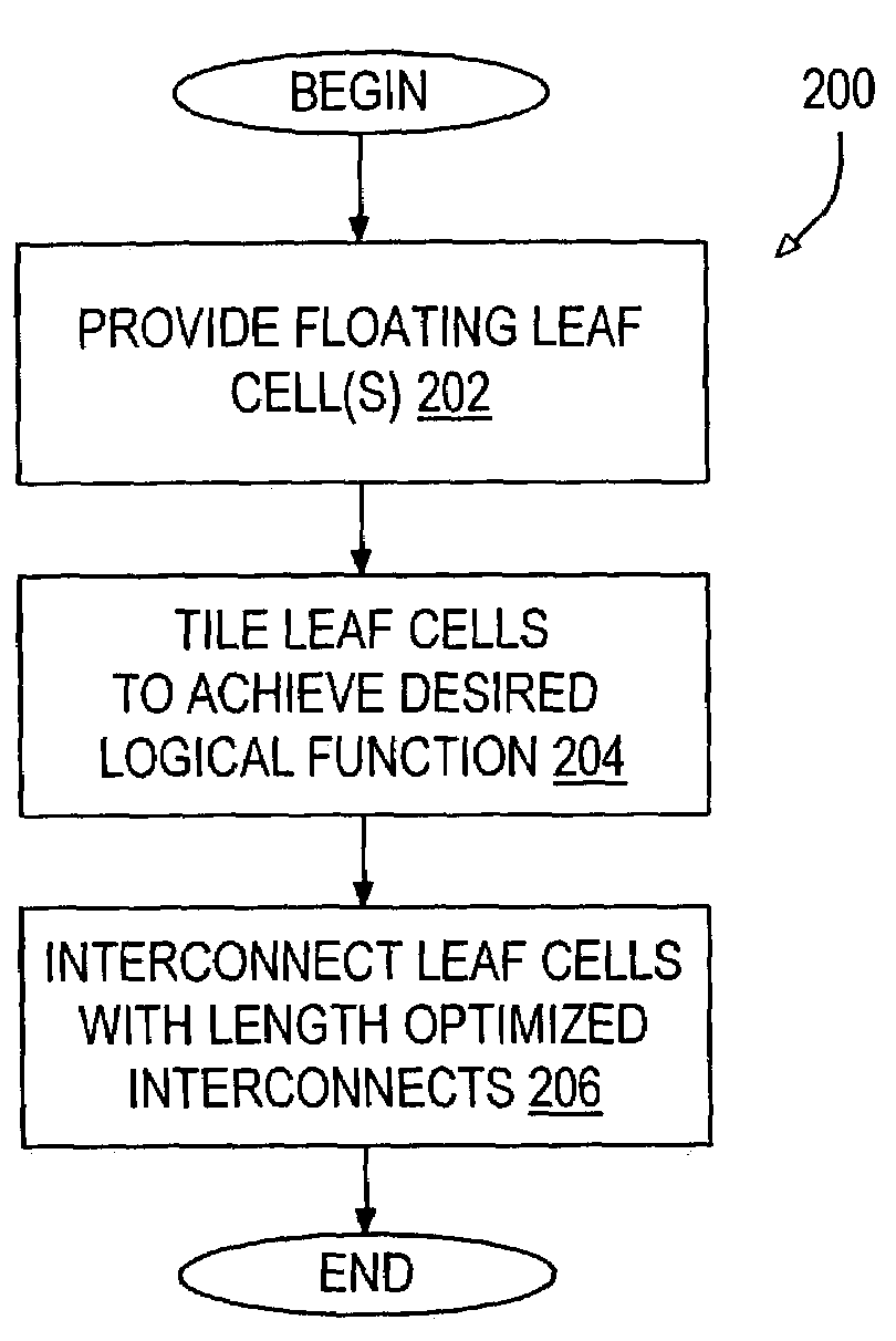
[0017]Generally speaking, the present invention encompasses a method for producing PLA circuits by leaf cell tiling in which the length of the interconnects are optimized based upon the implemented logical function. Input signals to and output signals from the “and plane” and “or plane” of a design are terminated at the point in the appropriate plane beyond which the signal is no longer required. In this manner, the average length of the interconnects in the PLA planes is shortened. The shorter interconnects have reduced parasitic capacitance that results in faster signal transitions (reduced delay) and lower power consumption.

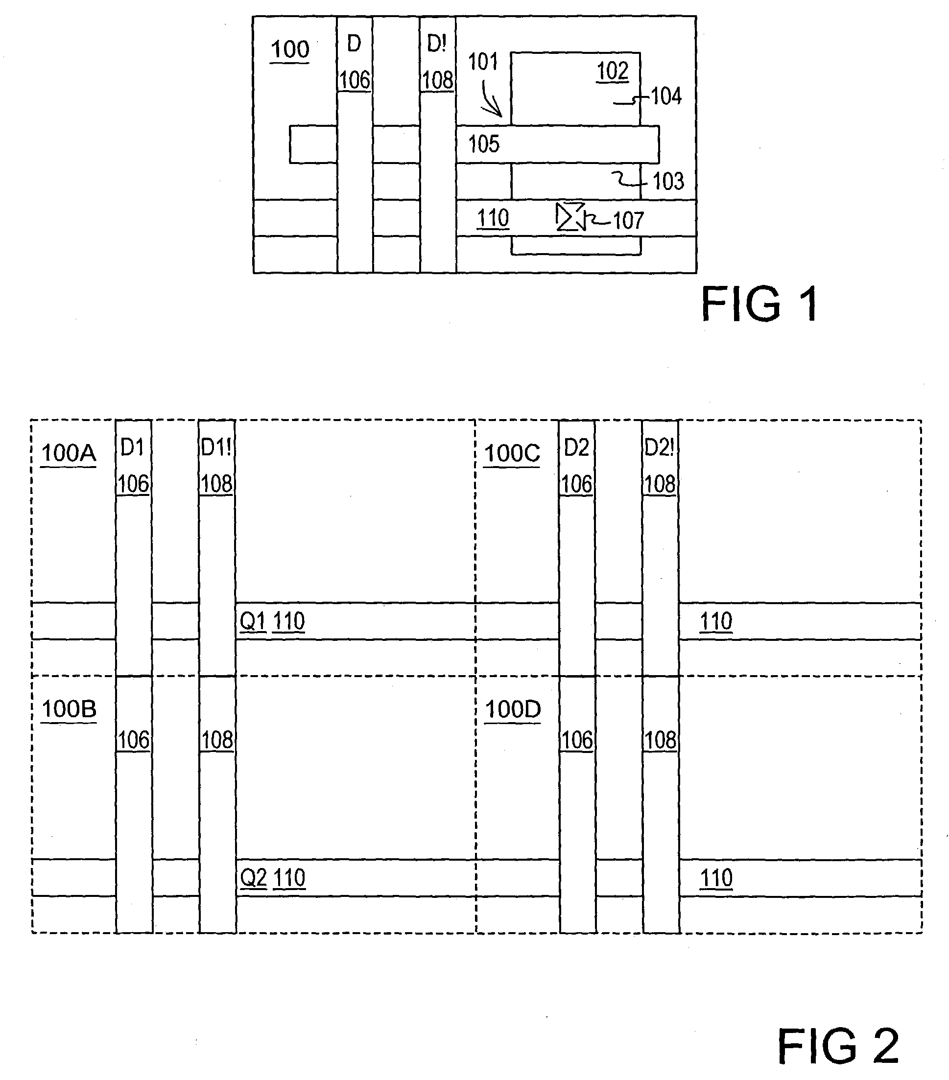
[0018]Turning now to the drawings, FIG. 1 illustrates a conventional cell (also referred to as a leaf cell) 100 suitable for use in an interconnection-by-abutment design. In this implementation, leaf cell 100 includes a transistor 101, which is typically n-type or n-mos, formed by the transistor gate 105 traversing a source / drain region 102 as will be familiar...


PUM


Abstract

A method of designing a logic circuit includes providing a leaf cell having at least one transistor. The leaf is suitable for use as a 1-cell or a 0-cell in the logic circuit. A first array of abutting leaf cells is tiled using at least one 1-cell and at least one 0-cell to define at least one logical expression by the relative positions of the array cells. Length optimized interconnects are added to the array. Each length optimized interconnect terminates at a last leaf cell in the array to which the interconnect makes contact. The leaf cell may be a floating leaf cell in which any pair of abutting cells are electrically isolated from one another until the length optimized interconnects are added to the design. The leaf cell array likely includes a set of rows and a set of columns in which the leaf cells in each row and the set of columns each correspond to an input of the logical expression.

Description

BACKGROUND[0001]1. Field of the Present Invention[0002]The present invention generally relates to the field of circuit design and more specifically to the field of programmable logic array circuit design.[0003]2. History of Related Art[0004]Programmable logic arrays (PLA's) are well known in the field of integrated circuits. A PLA typically includes an array of substantially identical cells where each cell includes one or more transistors and one or more interconnect elements. These cells may be placed as desired within a device. The individual cells can then be connected in a desired fashion using a customized contact layer, interconnect (metal) layer, or both to achieve a desired logical function. This type of design is particularly suitable for generating certain logic functions including a sum of products type of function. Using this technique enables manufacturers to produce customized logic with quick turnaround because wafers can be processed to the final interconnect layer. ...

Claims


Application Information

Patent Timeline
IPC IPC(8): G06F17/50H01L21/82H03K19/00H03K19/177
CPCG06F17/5054G06F30/34
Inventor BUCKI, ROBERT JOHNDHONG, SANG HOOSILBERMAN, JOEL ABRAHAMTAKAHASHI, OSAMU
Owner IBM CORP
Why Eureka
Try Eureka