Dense semiconductor fuse array

a fuse array and semiconductor technology, applied in the field of semiconductor structures, can solve the problems of affecting the overall size of circuit designs that incorporate such arrays, purely resistive fuse elements, and conventional fuse arrays that are not efficiently area-optimized, and achieve the effect of improving the density of the array

Active Publication Date: 2007-06-05
GLOBALFOUNDRIES US INC
View PDF17 Cites 11 Cited by
  • Summary
  • Abstract
  • Description
  • Claims
  • Application Information

AI Technical Summary

Benefits of technology

[0009]The present invention addresses the above-described problems by providing a dense semiconductor fuse array having common cathodes. Common cathodes improve array density. Also, depending on the fuse type, common cathodes can eliminate the need for an additional metal wiring layer. In accordance with one aspect of the invention, a dense semiconductor fuse array is provided having a plurality of column lines, a plurality of common cathodes, and a plurality of fuse elements where multiple fuse elements share a common cathode. Furthermore, each fuse of the dense semiconductor fuse array can comprise a diode for preventing secondary current paths. The diodes can be integrated into the fuse structures.

Problems solved by technology

First, conventional fuse arrays are not efficiently area-optimized.
In other words, conventional fuse arrays are not as densely arranged as possible, thereby negatively impacting the overall size of circuit designs that incorporate such arrays.
Additionally, conventional fuse arrays consisting of purely resistive fuse elements suffer from secondary currents that flow through a network of wires around the selected fuse.
The secondary currents make the programming and sensing of individual fuses difficult.

Method used


Image

  • Dense semiconductor fuse array
  • Dense semiconductor fuse array
  • Dense semiconductor fuse array

Examples


Embodiment Construction

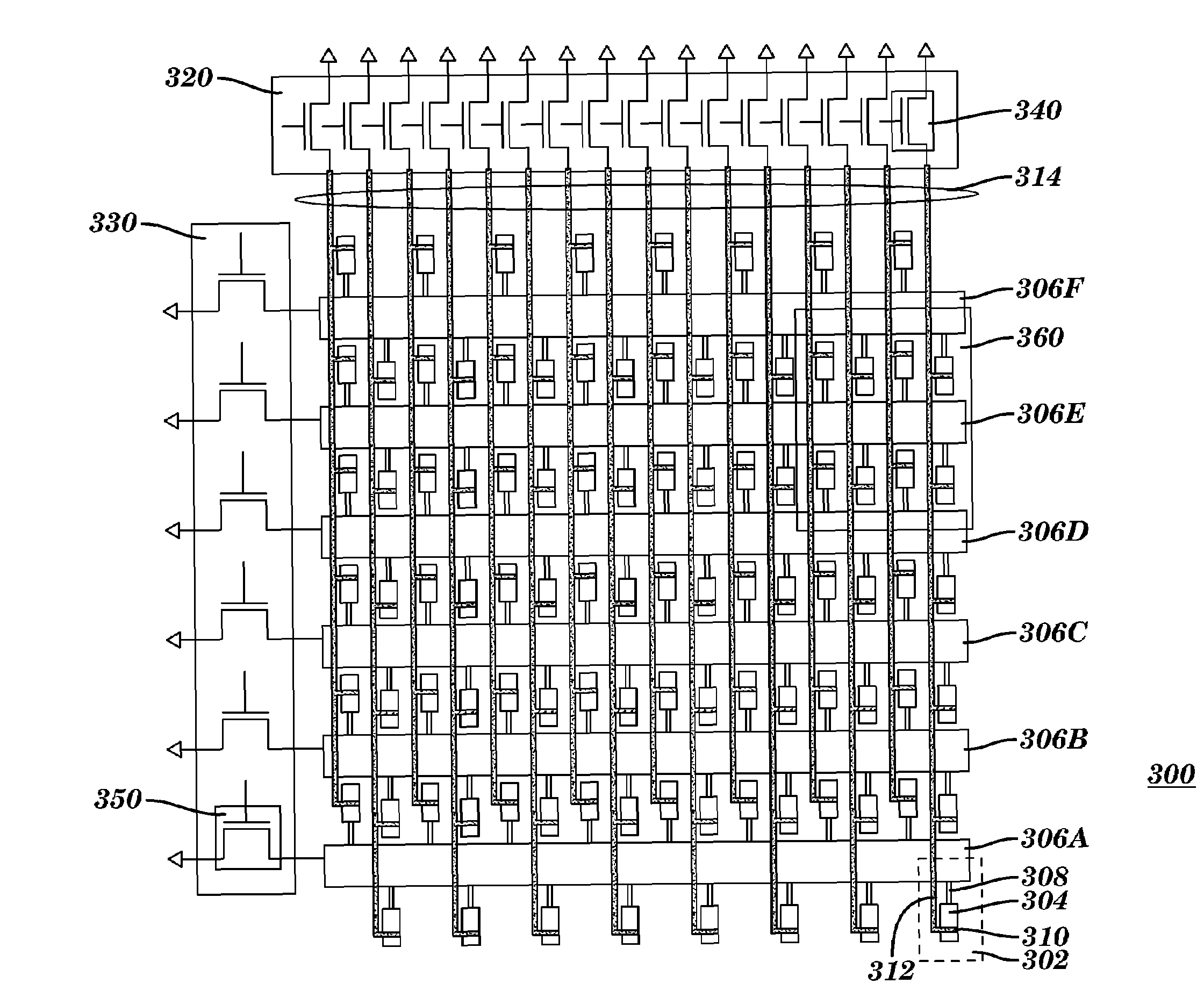
[0023]FIG. 3 illustrates a top-down view of the dense semiconductor fuse array according to an embodiment of the present invention. Dense semiconductor fuse array 300 is formed on a semiconductor substrate (not shown). The semiconductor substrate can comprise any suitable semiconductor material such as bulk silicon, silicon-on-insulator (“SOI”), SiGe, GaAs, or the like. For illustrative purposes only, dense semiconductor fuse array 300 is a 6×16 fuse array (six row lines by sixteen column lines). The dense semiconductor fuse array of the present invention can comprise any suitable number of row and column lines. Located at the intersection of each row and column line of dense fuse array 300 is a fuse. Each fuse comprises an individual anode, a common (i.e. shared) cathode, and an individual fuse link. For example, at the intersection of the sixth row line and the sixteenth column line of dense fuse array 300 is fuse 302. Fuse 302 comprises anode 304, common cathode 306A, and fuse li...


PUM


Abstract

The present invention provides a dense semiconductor fuse array having common cathodes. The dense semiconductor fuse array of the present invention occupies less area than conventional semiconductor fuse arrays, can comprise integrated diodic components, and can require only one metal wiring layer for making electrical connections to the fuse array.

Description

BACKGROUND OF THE INVENTION[0001]The present invention relates to semiconductor structures, and particularly, to dense semiconductor fuse arrays having common cathodes.[0002]Electrically operable fuses are utilized within the field of integrated circuit devices and processes for a number of purposes, including programming alterable circuit connections, or replacing defective circuit elements with redundant circuit elements. Electrically operable fuses are typically arranged in an array. Such fuse arrays typically comprise a number of fuses where each fuse can be individually selected and programmed. By activating a particular row and column of the fuse array, an individual fuse can be selected and programmed by driving sufficient current through the fuse, thereby causing it to heat up and eventually break. Once the fuse breaks, it can no longer pass current and is considered “programmed.”[0003]FIG. 1 illustrates a conventional fuse 100. Fuse 100 comprises anode 110, cathode 120 and ...

Claims


Application Information

Patent Timeline
Patent Type & Authority Patents(United States)
IPC IPC(8): H01L31/062H01L31/113
CPCG11C17/16H01L23/5256H01L27/10H01L2924/3011H01L2924/0002H01L2924/00
Inventor PARK, BYEONGJUKOTHANDARAMAN, CHANDRASEKHARANIYER, SUBRAMANIAN S.
Owner GLOBALFOUNDRIES US INC
Why Eureka
Try Eureka