Method of manufacturing semiconductor device

a manufacturing method and semiconductor technology, applied in the direction of semiconductor devices, basic electric elements, electrical equipment, etc., can solve the problems of difficult to achieve the reduction of programming voltage, which is required for increasing storage density, and the difficulty of increasing the existing storage density of flash memories, so as to eliminate the issue of “over-erasure”, reduce the size of the chip, and maintain the electrical isolation performance of the existing chip

Active Publication Date: 2013-12-12
SHANGHAI HUAHONG GRACE SEMICON MFG CORP
View PDF2 Cites 8 Cited by
  • Summary
  • Abstract
  • Description
  • Claims
  • Application Information

AI Technical Summary

Benefits of technology

[0006]The present disclosure addresses the drawback of the prior art by presenting a method of manufacturing a semiconductor device. The method can effectively reduce chip size and eliminate the issue of “over-erasure” while maintaining the existing in-chip electrical isolation performance. Additionally, the method can increase the memory array density of a memory device and prepare pick-up electrodes with ensured quality for both the memory device and other semiconductor devices. Moreover, the method can be effectively used in the manufacturing of a semiconductor device incorporating a split-gate structure and a MOS transistor which includes a desired thickness of gate oxide.
[0019]Every two bit cells of a semiconductor device constructed in accordance with the method discussed above co-share a single word line, thereby enabling performing programming activities, including reading, erasing and those performed by hot electron injection, to the bit cells by applying different operating voltages to the word line, two control gates and source / drain regions of the semiconductor device. The word line co-share configuration enables a split-gate type flash memory device to effectively reduce chip size and eliminate the issue of “over-erasure” while maintaining the existing chip electrical isolation performance. Moreover, the method is able to form pick-up electrodes for other semiconductor devices of the same chip without damaging or affecting pick-up electrodes of the memory device and without needing any additional processes or increasing process complexity. Furthermore, the method can be effectively used in the manufacturing of a semiconductor device incorporating a split-gate structure and a MOS transistor which includes a desired thickness of gate oxide.

Problems solved by technology

Whereas, due to the limitation in programming voltage, it is a great challenge to increase the existing storage density of flash memories by size shrinkage.
However, in this regard, limited by the structure of conventional flash memories, reducing the programming voltage, which is required for increasing the storage density, is difficult to achieve.
On the other hand, as a split-gate structure adopts an additional word line than a stacked-gate structure, it generally leads to a greater chip size.
This is unfavorable for producing a semiconductor memory device with densely packed memory cells and thus a high storage intensity which encourages the storage circuit layout to be designed as small as practicable.
Increasing the density of memory cells further raises the density of the metal wires and thus adds manufacturing difficulties because it requires extremely fine lines to be formed in relevant masking and etching processes.
Therefore, the method of increasing memory cell density by forming more memory cells in the wafer imposes critical requirements on manufacturing processes, which limits its applications.

Method used


Image

  • Method of manufacturing semiconductor device
  • Method of manufacturing semiconductor device
  • Method of manufacturing semiconductor device

Examples


Embodiment Construction

[0023]Exemplary embodiments are described in detail below in conjunction with the accompanying drawings so that this disclosure will be thorough and easily understood.

[0024]A method of manufacturing a memory device in accordance with preferred embodiments will be described in detail with reference to the accompanying drawings.

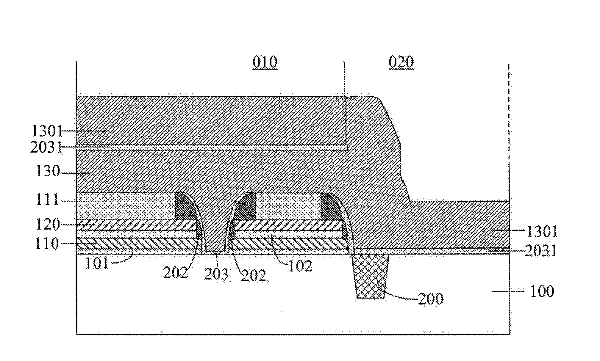
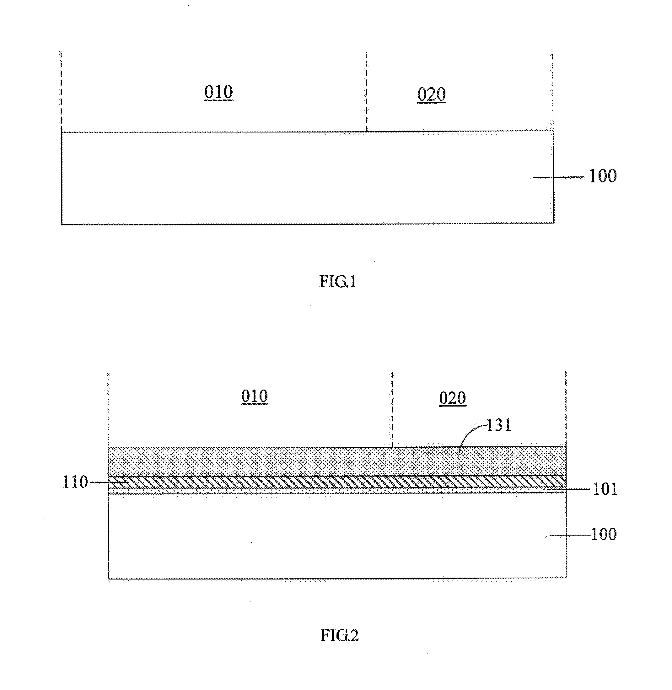
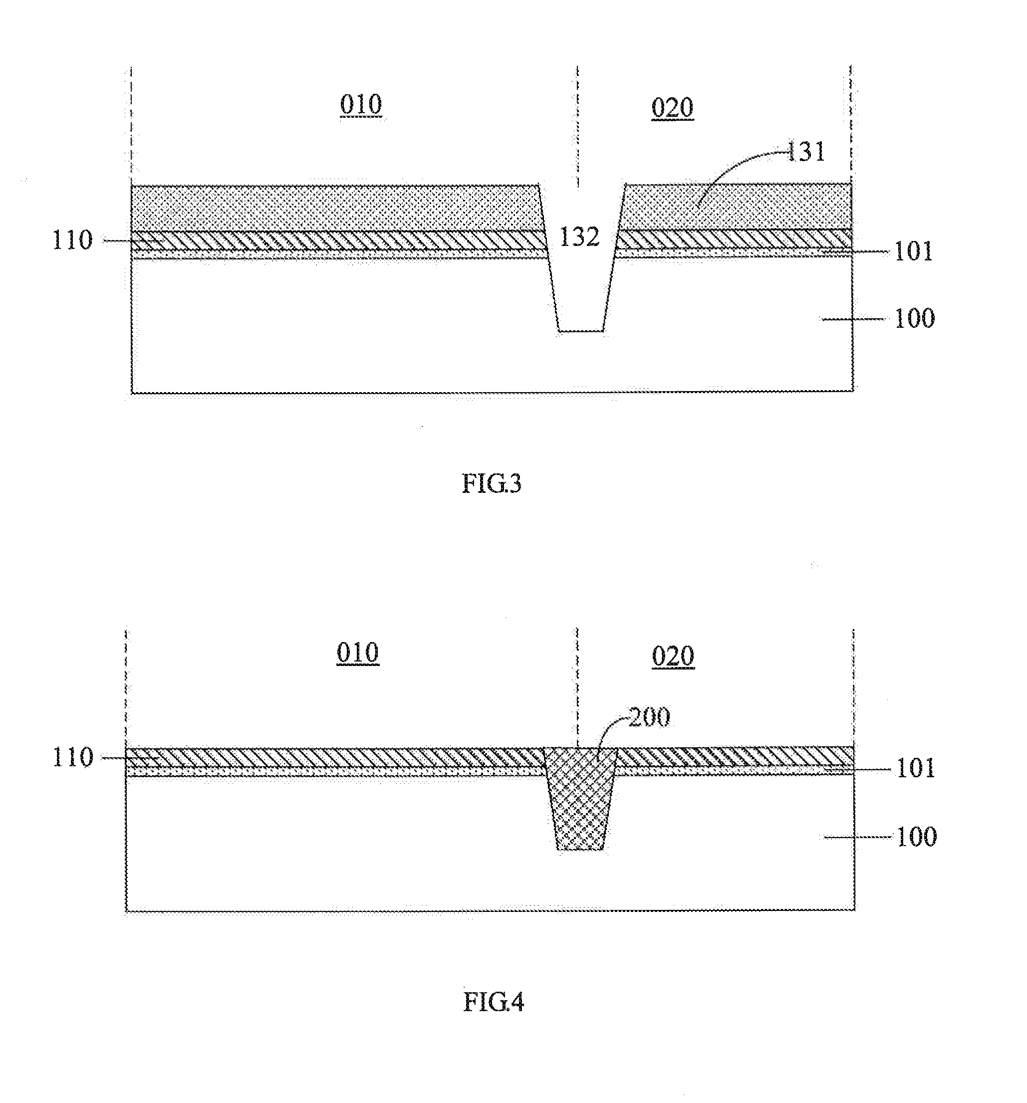
[0025]Turning now to FIG. 1, in a first step of the method, a semiconductor substrate 100 is provided. The semiconductor substrate 100 may typically be a silicon substrate or a silicon-on-insulator (SOI) substrate. The semiconductor substrate 100 includes a first device region 010 and a second device region 020.

[0026]Next, in a second step, a first dielectric layer 101, a first conductive layer 110, a second dielectric layer 102, a second conductive layer 120 and a first etch stop layer 111 are sequentially formed over the semiconductor substrate 100 in this order.

[0027]The first dielectric layer 101 may be a gate oxide layer typically comprised of silicon diox...


PUM


Abstract

A semiconductor device fabrication method particularly suitable for the fabrication of a 90 nm embedded flash memory is disclosed. The method includes: forming a dielectric layer having a first thickness over a first device region and forming a dielectric layer having a second thickness different from the first thickness over a second device region, the dielectric layer having a first thickness serving as a tunnel oxide layer of a split-gate structure, the dielectric layer having a second thickness serving as a gate oxide layer of a MOS transistor. The method enables the fabrication of a MOS transistor including a gate oxide layer with a desired thickness.

Description

CROSS-REFERENCES TO RELATED APPLICATIONS[0001]This application claims the priority of Chinese patent application number 201210191226.5, filed on Jun. 11, 2012, the entire contents of which are incorporated herein by reference.TECHNICAL FIELD[0002]The present invention relates in general to the fabrication of semiconductor devices, and more particularly, to a method of manufacturing a semiconductor device including a split-gate structure and a metal oxide semiconductor (MOS) transistor. The method is particularly suitable for use in the fabrication of a 90 nm embedded flash memory.BACKGROUND[0003]Flash memories have been focused in researches for non-volatile memory devices due to their advantages such as convenience to use, high storage density, and excellent reliability. Since the debut of the first flash memory in 1980s, flash memories have been widely used in cell phones, laptop computers, palm-sized computers, USB flash disks and other portable and communication devices, accompa...

Claims


Application Information

Patent Timeline
Patent Type & Authority Applications(United States)
IPC IPC(8): H01L29/66
CPCH01L29/66825H01L29/42328H01L29/7885H10B41/35
Inventor GU, JINGLI, BINGHAN
Owner SHANGHAI HUAHONG GRACE SEMICON MFG CORP
Why Eureka
Try Eureka