Image sensor package and its manufacturing method
- Summary
- Abstract
- Description
- Claims
- Application Information
AI Technical Summary
Benefits of technology
Problems solved by technology
Method used
Image

Examples
Embodiment Construction
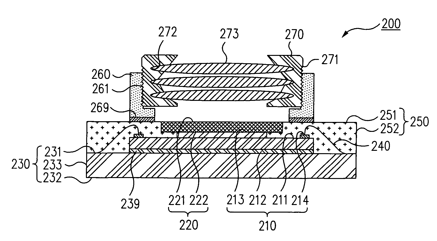
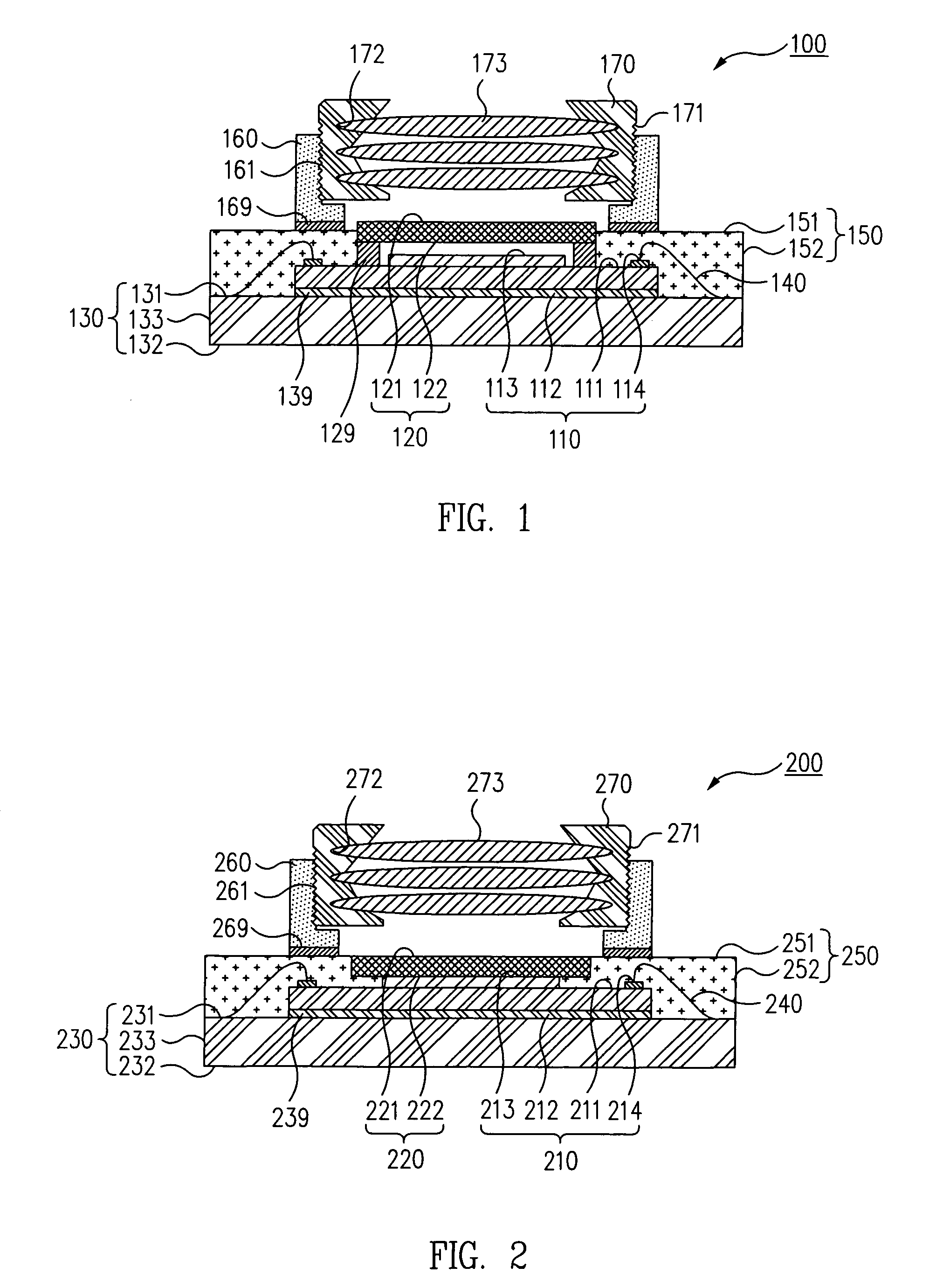
[0029]Referring to FIG. 1, an image sensor package 100 in accordance with an embodiment of the present invention is shown in section.
[0030]As shown in the drawing, the image sensor package 100 according to the present invention includes an image sensor die 110 for sensing an external image and converting it into an electrical signal, an infrared ray protection glass 120 seated on the image sensor die 110, a substrate 130 attached to the image sensor die 110, electrically conductive wires 140 for electrically connecting the image sensor die 110 and the substrate 130 to each other, an encapsulant 150 for encapsulating the image sensor die 110, the infrared ray protection glass 120, the substrate 130 and the electrically conductive wires 140 while exposing a defined region of the infrared ray protection glass 120 to the outside, a mount holder 160 adhered to a surface of the encapsulant 150, and a barrel 170 coupled to the inside of the mount holder 160 to appropriately focus the exter...
PUM
 Abstract
Description
Claims
Application Information
 - Generate Ideas
- Intellectual Property
- Life Sciences
- Materials
- Tech Scout
- Unparalleled Data Quality
- Higher Quality Content
- 60% Fewer Hallucinations
Browse by: Latest US Patents, China's latest patents, Technical Efficacy Thesaurus, Application Domain, Technology Topic, Popular Technical Reports.
© 2025 PatSnap. All rights reserved.Legal|Privacy policy|Modern Slavery Act Transparency Statement|Sitemap|About US| Contact US: help@patsnap.com