Method, system and computer program product for automatically estimating pin locations and interconnect parasitics of a circuit layout

a technology of interconnection parasitics and pin locations, applied in the field of vlsi circuit design, can solve the problems of affecting the design process, requiring significant manual effort on the part of the designer, and unable to consider the rc parasitic values as components,

Inactive Publication Date: 2007-06-05
GLOBALFOUNDRIES INC
View PDF5 Cites 27 Cited by
  • Summary
  • Abstract
  • Description
  • Claims
  • Application Information

AI Technical Summary

Benefits of technology

[0007]Systems and computer program products corresponding to the above-summarize methods are also described and claimed herein.
[0008]Further, additional features and advantages are realized through the techniques of the present invention. Other embodiments and aspects of the invention are described in detail herein and are considered a part of the claimed invention.

Problems solved by technology

Connection paths for signals between different components of a VLSI circuit have inherent RC values that may cause delays in propagation.
This process requires significant manual effort on the part of the designer in measuring and estimating the wire lengths between circuit components in the design, and then annotating the schematic with these parasitic electrical elements.
This manually intensive process further makes it difficult to consider the RC parasitic values as components are moved or different configurations are explored, since the parasitic values would need to be recalculated.
Another drawback to this design method is that the design effort is relatively far along before RC parasitic delays are considered, making it difficult to revise a design to overcome a negative impact of such RC parasitic delays.

Method used


Image

  • Method, system and computer program product for automatically estimating pin locations and interconnect parasitics of a circuit layout
  • Method, system and computer program product for automatically estimating pin locations and interconnect parasitics of a circuit layout
  • Method, system and computer program product for automatically estimating pin locations and interconnect parasitics of a circuit layout

Examples


Embodiment Construction

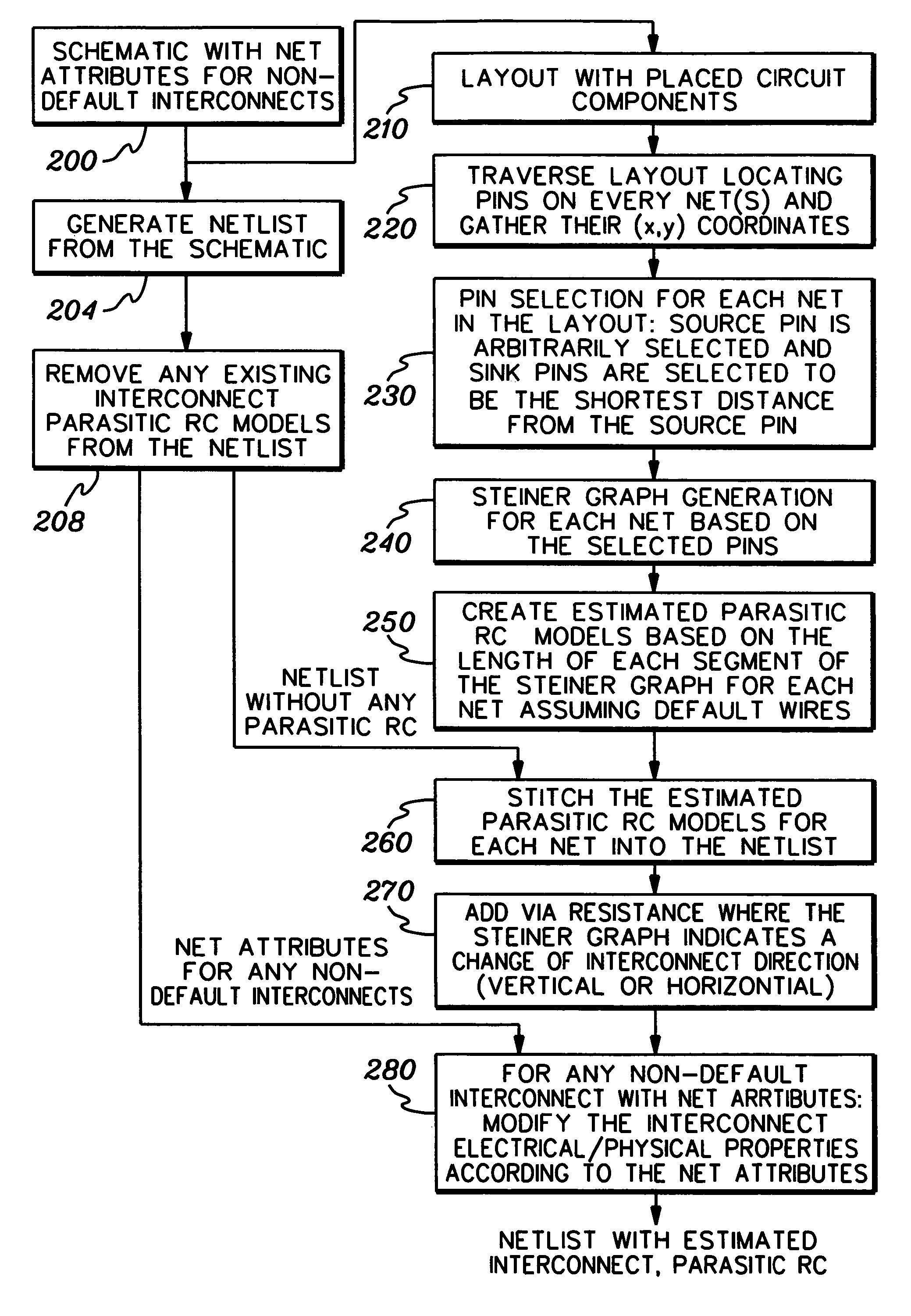
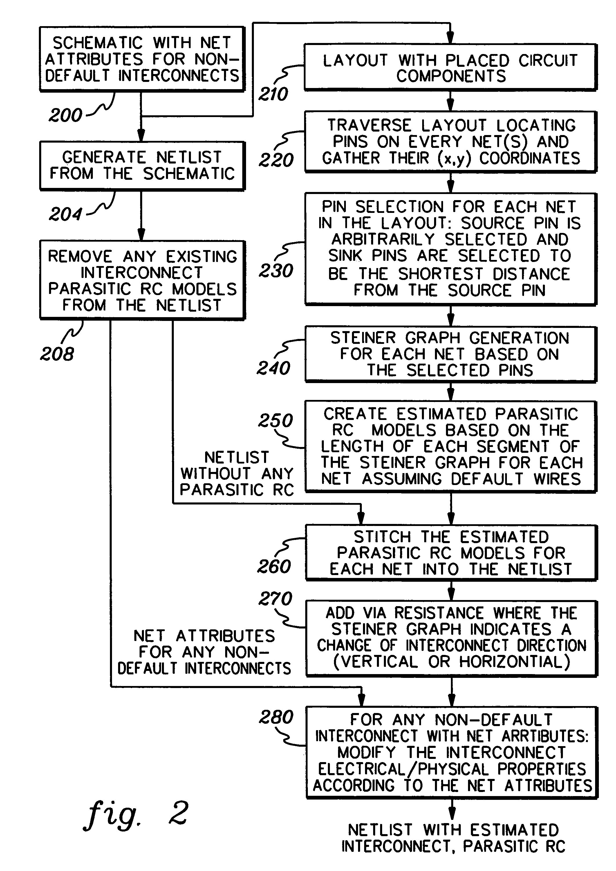
[0020]As briefly noted, in custom VLSI circuit design, the interconnect parasitic (either wire or via) between circuits in a design is typically manually measured or estimated based on a drawn floorplan of the design. These interconnect parasitic elements are then manually annotated onto the schematic. The schematic with the estimated interconnect parasitics is then analyzed through timing tools for timing and area optimization. The process requires significant manual effort on the part of the designer in measuring and estimating wire lengths between circuits in the design and then annotating the schematic with these parasitic elements. The accuracy and completeness of the estimated interconnect lengths between circuits depends upon the experience of the designer and can vary significantly within a large VLSI design team. Because of the time required, typically only a critical portion of the interconnect lengths are estimated, and thus, the timing of the design will not be known wit...


PUM


Abstract

A circuit design technique is provided for automatically estimating lengths of interconnect segments to be employed in interconnecting at least some circuit components of a plurality of placed circuit components of a circuit layout. The automatically estimating includes automatically generating pin locations for a plurality of pins in at least one level of the hierarchy to be employed with the at least some circuit components of the circuit layout, wherein the interconnect segments interconnect the plurality of pins. A route estimator is employed to estimate lengths of the interconnect segments based on the pin locations of the plurality of pins. The estimated interconnect segment lengths are then employed in automatically estimating resistance capacitance interconnect parasitics for the interconnect segments to be employed in the circuit layout.

Description

TECHNICAL FIELD[0001]This invention relates in general to VLSI circuit design, and more particularly, to an automated technique for estimating pin locations and lengths of interconnect segments to be employed in interconnecting at least some circuit components of a plurality of placed circuit components of a circuit layout, and for employing the estimated pin locations and interconnect segment lengths in estimating resistance capacitance interconnect parasitics for the circuit layout.BACKGROUND OF THE INVENTION[0002]In a large scale VLSI circuit design project, an initial step is to create a description of chip functionality. This description is created in Register Transfer Language (“RTL”). One of the considerations in a circuit design is to optimize the resistance capacitance (RC) values of the configuration, while minimizing the negative effects that the RC values may have on timing. Connection paths for signals between different components of a VLSI circuit have inherent RC valu...

Claims


Application Information

Patent Timeline
Patent Type & Authority Patents(United States)
IPC IPC(8): G06F17/50
CPCG06F17/5031G06F30/3312
Inventor CHAN, YIU-HINGCHU, JONATHAN M.
Owner GLOBALFOUNDRIES INC
Why Eureka
Try Eureka