Area efficient implementation of small blocks in an SRAM array

a technology of sram array and array block, applied in the field of area efficient implementation of sram array array block, can solve the problems of increasing power dissipation, increasing latency and dynamic power, and significant amount of additional power distribution switching circuitry, so as to improve device performance, reduce pitch, and minimize variations

Active Publication Date: 2007-06-26
TEXAS INSTR INC
View PDF5 Cites 55 Cited by
  • Summary
  • Abstract
  • Description
  • Claims
  • Application Information

AI Technical Summary

Benefits of technology

[0015]In yet another aspect of the present invention, the dummy cell (second) layout configuration, comprises an SRAM cell configuration (e.g., a 6T cell configuration) having two transistor pairs, each pair comprising an NMOS and a PMOS transistor, wherein the gates of the four transistors and the PMOS drains are connected to a single node, and wherein the drain terminals of the PMOS and NMOS transistor in each respective inverter are not connected to one another, thereby avoiding a crowbar current within each inverter when supply voltages applied to the first and second pair of power supply voltage lines are different. Either, or both of the power supply lines (e.g., Vss, Vdd) may be raised or lowered in the dummy cell structure to accomplish the power supply isolation between the array segments.
[0019]Fabrication of the array and dummy cell structures in accordance with the present invention, moreover, may also advantageously achieve significantly minimized variations from the desired feature sizing and a corresponding improvement in device performance (e.g., static Iddq (off-state leakage current), and yield roll-off with decreasing pitch) by comparison to those using special boundary-effect OPC considerations.

Problems solved by technology

As transistor feature sizes are continually reduced, however, achieving good, consistent cell patterning that maintains this transistor matching to avoid increased power dissipation is becoming more difficult in SRAM, despite the use of optical pattern correction (OPC) in the photolithographic process.
However, the switching between the rows of such an array configuration would add latency and dynamic power.
Another problem with this solution is that a significant amount of additional power distribution switching circuitry and wafer real estate must be provided to isolate the power lines between each row of the entire array.
However, segmenting an array into these relatively small groups of rows may result in inconsistent patterning of the edge rows relative to rows central to the array, and may require significantly more peripheral decoder circuitry and the associated additional area penalty.

Method used


Image

  • Area efficient implementation of small blocks in an SRAM array
  • Area efficient implementation of small blocks in an SRAM array
  • Area efficient implementation of small blocks in an SRAM array

Examples


Embodiment Construction

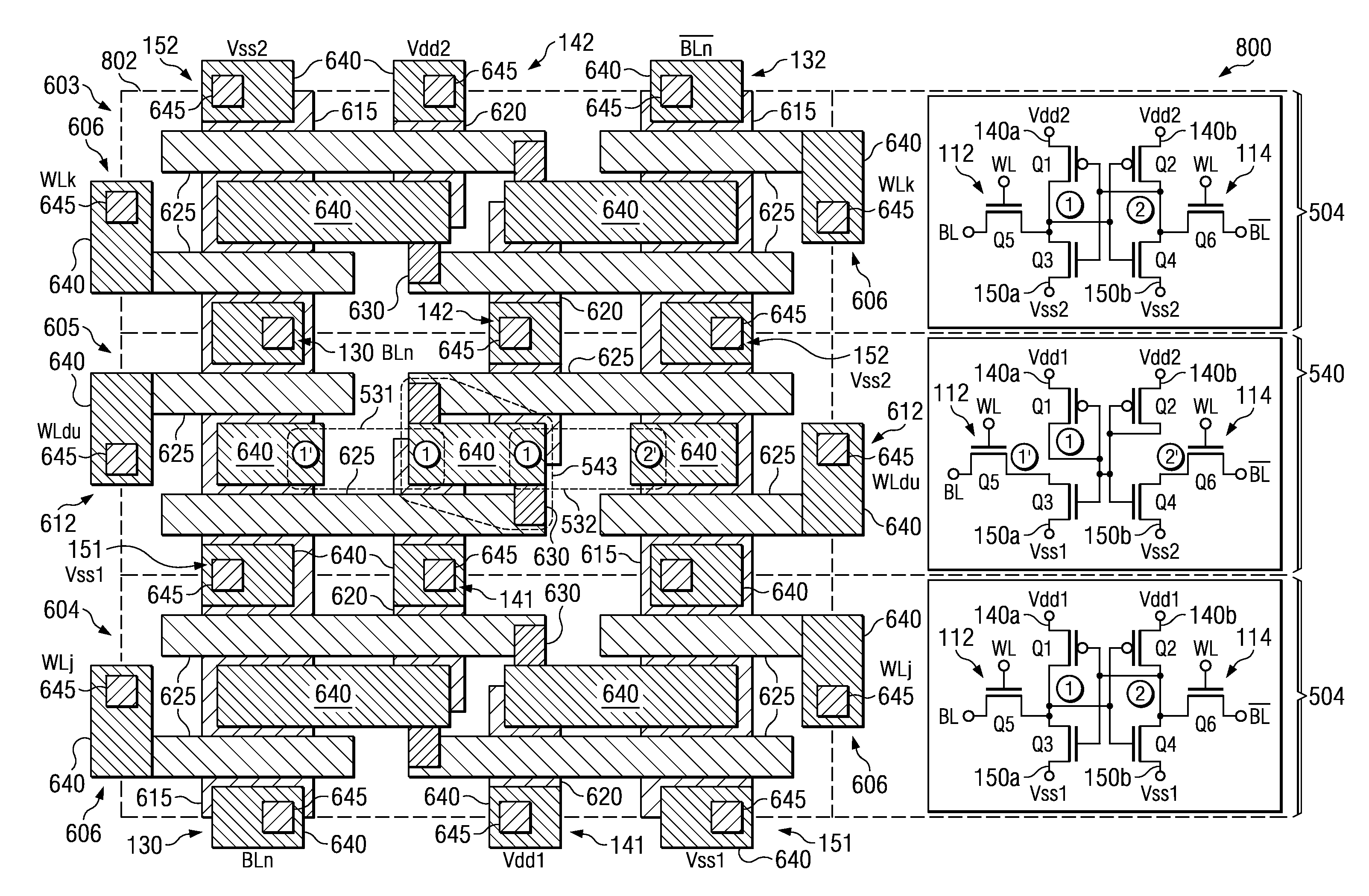
[0038]The present invention will now be described with reference to the attached drawings, wherein like reference numerals are used to refer to like elements throughout. The invention provides an array structure used for segmenting an array into smaller array blocks, wherein a dummy cell row structure is used to isolate the power supply lines of the array segments on either side of the dummy cell row. The dummy cell structure avoids the use of special OPC conditions at the power supply line and block boundaries by maintaining substantially the same pattern and uniformity as the adjacent cell rows at the lower patterning levels. The dummy cell may be slightly different from the operational cell in the various pattern levels so long as the difference in the dummy cell pattern does not significantly affect the operational cell. In particular, the patterns in the dummy cell may be more significantly different at the M1 and upper metal layers to avoid crowbar currents within and between ...


PUM


Abstract

An SRAM array with a dummy cell row structure in which the SRAM array is divided into segments isolated by a row pattern of dummy cells. The dummy cell structure provides a continuous cell array at the lower cell patterning levels. The SRAM array includes a first and second array block each including an SRAM cell having a first layout configuration, one or more of the dummy cells having a second layout configuration arranged along the row pattern associated with a wordline of the SRAM array, a first power supply voltage line connected to the first array block, and a second different power supply voltage line connected to the second array block. The first and second power supply voltage lines of the array blocks are further connected to the one or more dummy cells.

Description

FIELD OF INVENTION[0001]The present invention relates generally to semiconductor memory devices, and more particularly to structures for segmenting an SRAM array into smaller array blocks using one or more rows of dummy cells of the array for isolating supply lines to the array blocks in the manufacture of semiconductor products.BACKGROUND OF THE INVENTION[0002]Current trends in the semiconductor and electronics industry require memory devices to be made smaller, faster and require less power consumption. One reason for these trends is that more personal devices are being manufactured that are relatively small and portable, thereby relying on battery power. In addition to being smaller and more portable, personal devices are also requiring increased memory and more computational power and speed. In light of all these trends, there is an ever increasing demand in the industry for smaller, faster, and lower power dissipation memory cells and transistors used to provide the core functi...

Claims


Application Information

Patent Timeline
Patent Type & Authority Patents(United States)
IPC IPC(8): G11C11/34
CPCG11C11/412H01L27/11H01L27/1104H10B10/00H10B10/12
Inventor HOUSTON, THEODORE W.SCOTT, DAVID BARRYTHIRUVENGADAM, SUDHA
Owner TEXAS INSTR INC
Why Eureka
Try Eureka