Mark for visual inspection upon assembling a display

a visual inspection and display technology, applied in the direction of identification means, instruments, non-linear optics, etc., can solve the problems of poor effect of injected current value, connection failure, and difficulty in perfect positioning of each lead disposed with high density, so as to achieve effective inspection work

Inactive Publication Date: 2007-06-26
TOHOKU PIONEER CORP
View PDF8 Cites 9 Cited by
  • Summary
  • Abstract
  • Description
  • Claims
  • Application Information

AI Technical Summary

Benefits of technology

[0021]That is, the conventional alignment marks are provided at the connecting portion of each substrate for positioning when connecting the panel substrate, the tape automated bonding substrate, and the flexible substrate each other, but can not be employed as marks for the visual inspection for checking the connection failure after connecting them since the alignment marks are too small. On the other hand, the marks for the visual inspection of the present invention enlarge the positional deviation which may occur at the connecting region in the longitudinal direction after the connection to enable the positional deviation to be converted into the deviation of the pair of marks for the visual inspection. In short, since the connection failure is checked by the enlarged deviation of the marks for the visual inspection while the deviation of the connecting region itself is delicate by just the sense of sight, the inspection objects sent to the microscope inspection process can be decreased, so that the effective inspection work can be caused.
[0022]Such a function of the marks for the visual inspection can be accomplished based on that the marks are formed a preset distance apart from the connecting region at each connecting portion of the panel substrate, the tape automated bonding substrate, and the flexible substrate, in the longitudinal direction. Since the marks for the visual inspection are located at such a position, the delicate angular deviation between the substrates to be connected can be converted into a large deviation amount in a direction perpendicular to the longitudinal direction to recognize the positional deviation at the connecting portion through enlarging it. In addition, since the marks for the visual inspection are provided in a lateral symmetry to the connecting portion, the direction and the amount of the deviation enable the angular deviation at the connecting portion to be further clearly recognized.

Problems solved by technology

Even if the positioning is performed by using the above-mentioned alignment marks and image processing of the alignment marks through the image pickup device, it is very difficult to perform perfect positioning of each lead disposed with high density since there may be any problem of resolution ability in a photographic image, or any formation error of a substrate glass, the TAB substrate, the FPC, and the like, respectively.
In addition, a positional deviation or a pressure-bonding failure may occur in the temporary bonding step or the permanent bonding step after the positioning is performed, so that a connection failure may be caused.
In particular, in the case of a display panel comprising current injection type display elements such as an organic EL display panel, a minute positional deviation causes a contact area formed by connected leads to be decreased, so that there may occur a bad effect to the injected current value.
Specifically, even if the connection between each lead is secured, the display performance may be deteriorated due to reduction of the contact area.
However, it is impossible for the visual inspection to perfectly examine to see whether the contact area between the leads is under a good or bad condition.
In addition, the above-mentioned alignment marks also for regulating the position of the both substrates are too small to find the inferior products by the visual inspection.
As a result, the workload in the microscopic inspection step can not be reduced.

Method used


Image

  • Mark for visual inspection upon assembling a display
  • Mark for visual inspection upon assembling a display
  • Mark for visual inspection upon assembling a display

Examples


Embodiment Construction

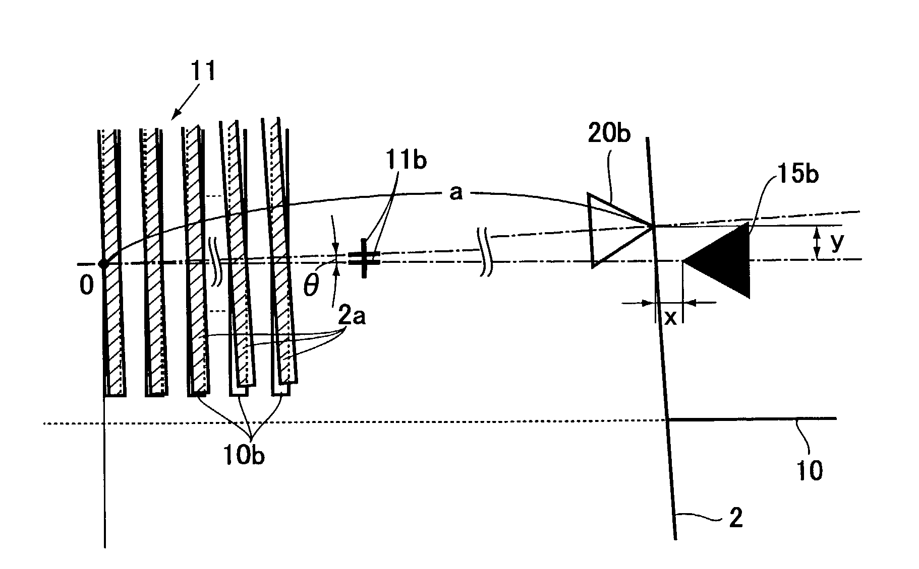
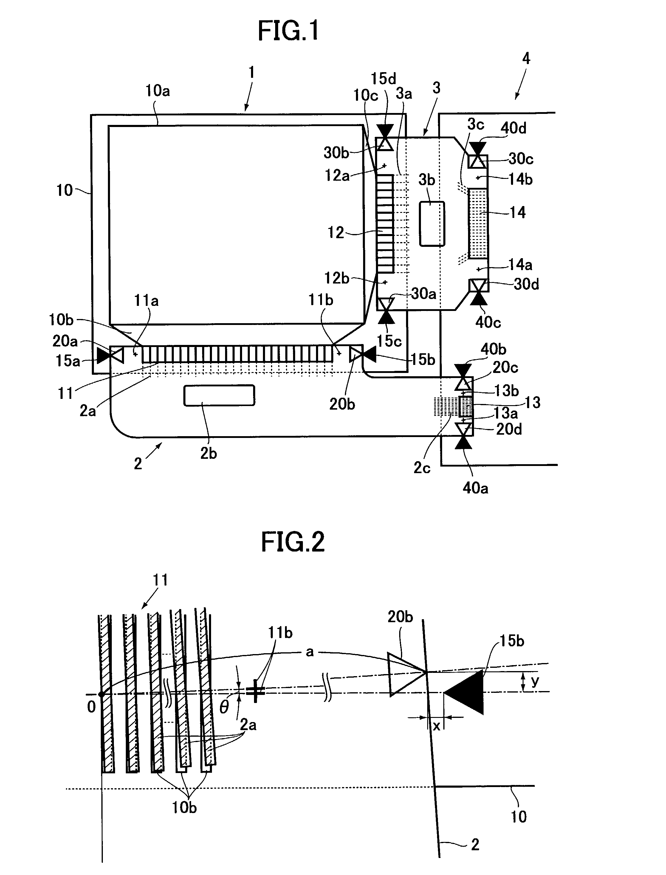
[0029]FIG. 1 is an explanatory view showing one embodiment of the present invention, with regard to mounting electronic parts on a display panel. An organic EL display panel 1, TAB substrates 2, 3, and a flexible substrate 4 are shown in the drawing.

[0030]In a panel substrate 10 of the organic EL display panel 1, leads 10b, 10c are drawn out as signal lines from a display area 10a. These leads 10b, 10c are respectively converged, and connected with each lead 2a, 3a of the TAB substrates 2, 3 at each connecting region 11, 12. Driving integrated Circuits 2b, 3b are mounted on the TAB substrates 2, 3, respectively.

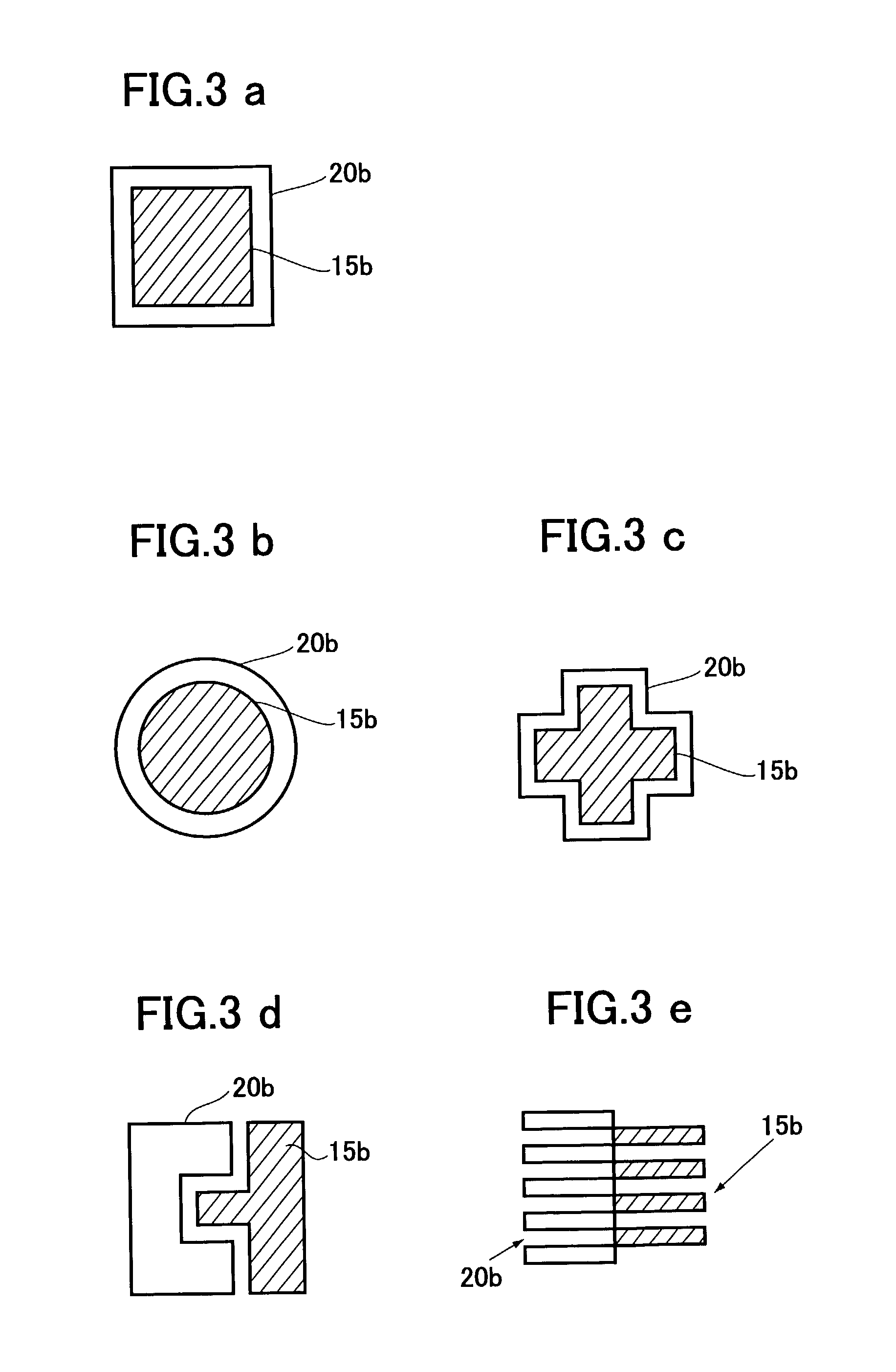
[0031]Leads 2c, 3c of the TAB substrates 2, 3 existing at a side of the flexible substrate 4 are connected to connecting lines of the flexible substrates 4 at connecting regions 13, 14 on the flexible substrate 4. In the neighborhood of the connecting regions 11, 12, 13, and 14, alignment marks 11a, 11b, 12a, 12b, 13a, 13b, 14a, and 14b are provided on the panel substrate 10,...


PUM

PropertyMeasurementUnit
flexibleaaaaaaaaaa
distanceaaaaaaaaaa
angleaaaaaaaaaa

Abstract

In the neighborhood of each connecting region of a panel substrate, tape automated bonding (TAB) substrates, and a flexible substrate, marks for a visual inspection are provided at a preset distance apart from the connecting region. According to the present marks, inferior products are eliminated with a high rate of accuracy upon visual inspection after completing a connection of display panel.

Description

BACKGROUND OF THE INVENTION[0001]1. Field of the Invention[0002]The present invention relates to a mark for a visual inspection upon assembling a display, and also to an electronic equipment provided with a display panel, a tape automated bonding (TAB) substrate, or a flexible substrate having the mark for the visual inspection thereon, respectively.[0003]The present application claims priority from Japanese Patent Application No. 2001-279532, the disclosure of which is incorporated herein by reference for all purposes.[0004]2. Description of the Related Prior Art[0005]Recently, a portable telephone or a personal digital assistant (PDA) has come into wide use, and needs a display panel which has a small size, reduced thickness, and high display capability. A liquid crystal display panel or an organic electro-luminescent (EL) display panel is employed as the display panel meeting with the requirement.[0006]In order to improve the display capability of such a display panel, an optical...

Claims


Application Information

Patent Timeline
Patent Type & Authority Patents(United States)
IPC IPC(8): G06K9/00G02F1/1345G01R31/04G09F9/00H01L21/60H01L51/50H05B33/12H05K1/02H05K3/00H05K3/36H05K13/08
CPCG01R31/043H05K3/361H05K1/0269H05K2201/09781H05K2201/09918H05K2203/166G01R31/68G09F9/00
Inventor OHAZAMA, HIDETAKA
Owner TOHOKU PIONEER CORP
Why Eureka
Try Eureka