Semiconductor device for rectifying memory defects

a semiconductor and memory technology, applied in the field of semiconductor devices, can solve the problems of increasing the number of masks and additional steps, increasing manufacturing costs, etc., and achieve the effects of high manufacturing cost, small area penalty, and high performance and high value-added semiconductors

Active Publication Date: 2007-07-03
SEMICON ENERGY LAB CO LTD
View PDF8 Cites 29 Cited by
  • Summary
  • Abstract
  • Description
  • Claims
  • Application Information

AI Technical Summary

Benefits of technology

[0014]Among the aforementioned four means, three means that are the first memory means, the rectifier means and the inspection means are formed over the same substrate while the second memory means is connected to a connecting terminal of the substrate. Alternatively, all of the four means are provided over the same substrate. Accordingly, a compact, thin and lightweight semiconductor device can be provided.
[0024]According to the invention which uses a flip-flop group as an inspection means, data of a defective memory cell can be written to a holding means with a simple method, thus a defect in the first memory means can be rectified with a simple method. Accordingly, the high-capacity and reliable first memory means can be provided.

Problems solved by technology

When a ferroelectric film is used, the number of masks and additional steps, and manufacturing cost are inevitably increased.

Method used


Image

  • Semiconductor device for rectifying memory defects
  • Semiconductor device for rectifying memory defects
  • Semiconductor device for rectifying memory defects

Examples


embodiment mode 1

[Embodiment Mode 1]

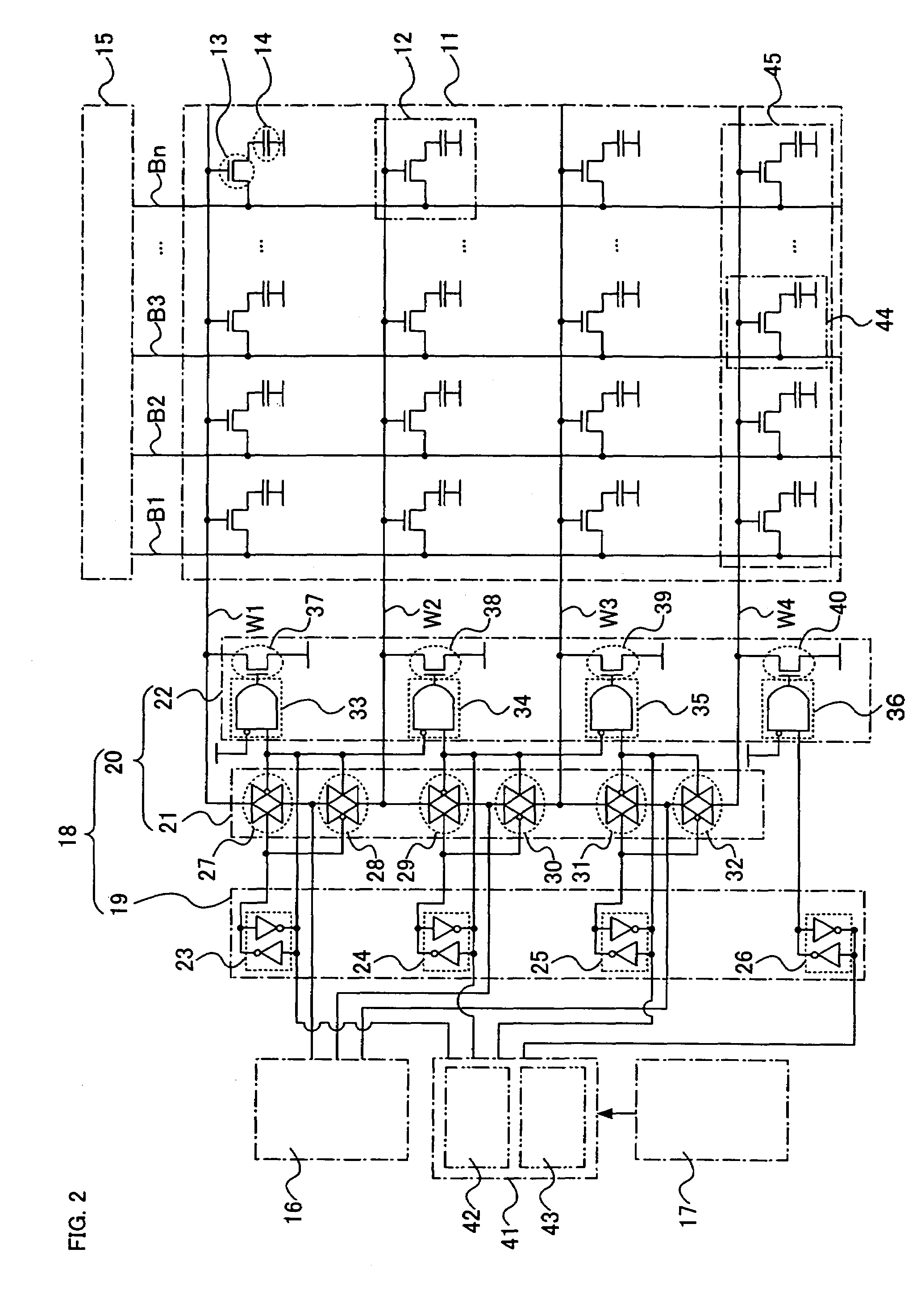
[0032]A semiconductor device in accordance with the invention comprises four primary components: a first memory means 101 (also referred to as a first memory circuit) including a memory cell and a redundant memory cell each including a memory element in the region where a bit line and a word line cross each other with an insulator interposed therebetween, a second memory means 102 (also referred to as a second memory circuit) for storing an address of a defective memory cell in the first memory means, a rectifier means 103 (also referred to as a rectifier circuit) and an inspection means 104 (also referred to as an inspection circuit) (see FIG. 1A).

[0033]The rectifier means 103 includes a holding means 105 (also referred to as a holding circuit) and a replacement means 106 (also referred to as a replacement circuit). The inspection means 104 includes a means for writing data of the second memory means 102 to the holding means 105. Further, the replacement means 10...

embodiment mode 2

[Embodiment Mode 2]

[0053]A semicoducter device in accordance with the invention comprises four primary components: a first memory means including a memory cell and a redundant memory cell each including a memory element in the region where a bit line and a word line cross each other with an insulator interposed therebetween, a second memory means for storing an address of a defective memory cell in the first memory means, a rectifier means and an inspection means.

[0054]The rectifier means includes a holding means and a replacement means. The inspection means includes a means for writing data of the second memory means to the holding means. Further, the replacement means including a means for replacing the function of the defective memory cell with the redundant memory cell.

[0055]More specifically, the replacement means includes a selection means for selecting only a bit line or a word line of the address where a redundant memory cell is disposed and for unselecting a bit line or a w...

embodiment mode 3

[Embodiment Mode 3]

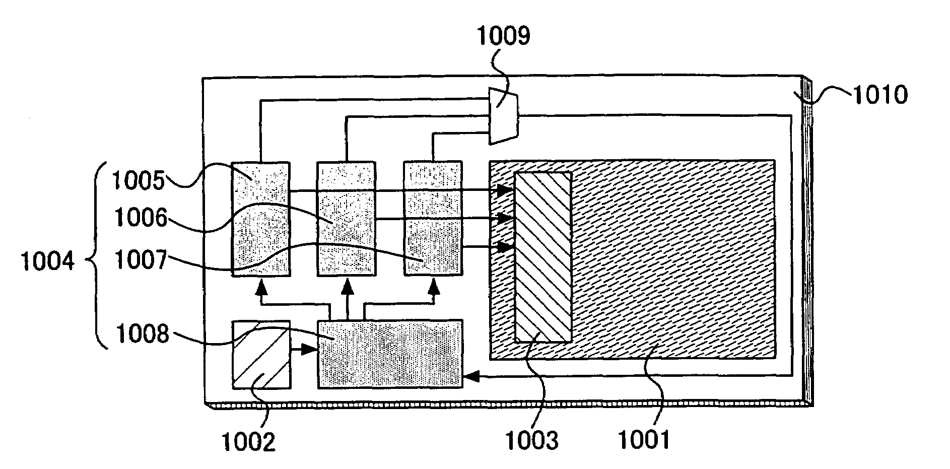
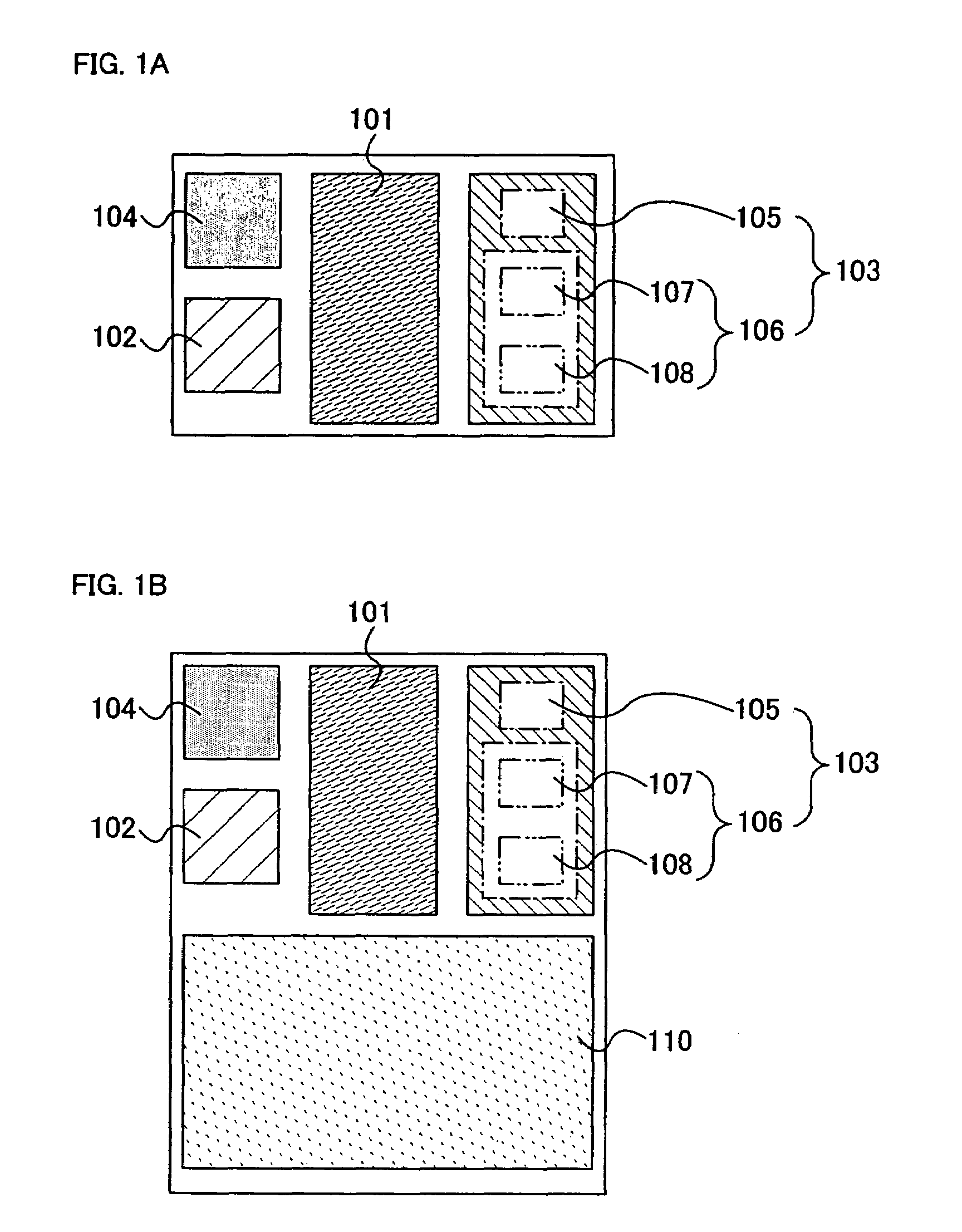
[0076]Description is made now on one embodiment mode of the invention with reference to the drawings. Referring to FIGS. 4A and 4B, a panel in which a pixel portion, a driver circuit for controlling the pixel portion, a memory and a CPU are all mounted over the same surface is described.

[0077]FIG. 4A shows a perspective view of a panel which comprises a substrate 406 over which are formed a pixel portion 401 including a plurality of pixels in a matrix array and driver circuits 402 and 403 on the periphery of the pixel portion 401. The panel also comprises a memory means 404 which corresponds to a VRAM (Video Random Access Memory), a RAM or a ROM, and a CPU 405. The panel further comprises an input terminal 409 to be supplied with signals for controlling the driver circuits 402 and 403, the memory means 404 and the CPU 405. The input terminal 409 is supplied with signals such as video signals and potentials via a tape 408. A sealing member (not shown) is provided s...


PUM


Abstract

The present invention provides a high-capacity and reliable semiconductor device which does not require additional circuits for use at power ON / OFF, additional steps nor high manufacturing cost, and which has a rectifier means for rectifying a defect easily. A semiconductor device comprises a first memory means including a memory cell and a redundant memory cell each including a memory element in the region where a bit line and a word line cross each other with an insulator interposed therebetween, a second memory means for storing an address of a defective memory in the first memory means, a rectifier means including a holding means and a replacement means, and an inspection means for writing data of the second memory means to the holding means. The replacement means replaces the defective memory cell with the redundant memory cell. In addition to the aforementioned four means, a display means for displaying images is provided as well.

Description

BACKGROUND OF THE INVENTION[0001]1. Field of the Invention[0002]The present invention relates to a semiconductor device comprising a plurality of blocks. More particularly, the invention relates to a semiconductor device comprising at least two blocks that are a memory means and a rectifier means for rectifying a defect in the memory means.[0003]2. Description of the Related Art[0004]One-chip semiconductor devices each comprising a plurality of blocks (also referred to as system LSIs) have been actively developed. Recently, higher integration of semiconductor devices as well as the manufacture of readable / writable memory means (also referred to as a memory or a RAM) is under development in accordance with the demand for further downsizing and higher performance of the devices. Such a memory means is required to have high capacity and reliability.[0005]As a method for rectifying defects of a semiconductor device, there is the mainstream technique of replacing a defective memory cell ...

Claims


Application Information

Patent Timeline
Patent Type & Authority Patents(United States)
IPC IPC(8): G11C29/00G01R31/28G11C7/00G11C7/20
CPCG11C7/20G11C29/781
Inventor MUTAGUCHI, KOHEI
Owner SEMICON ENERGY LAB CO LTD
Why Eureka
Try Eureka