Techniques for combining volatile and non-volatile programmable logic on an integrated circuit

a technology of programmable logic and integrated circuit, which is applied in the direction of pulse technique, instruments, computation using denominational number representation, etc., can solve the problems of limiting process selection, prohibitive non-volatile memory, and large field programmable gate arrays (fpgas) that contain on-chip volatile memory blocks that require a considerable amount of time to be configured at power-up

Inactive Publication Date: 2007-07-10
ALTERA CORP
View PDF25 Cites 25 Cited by
  • Summary
  • Abstract
  • Description
  • Claims
  • Application Information

AI Technical Summary

Benefits of technology

[0007]The logic in the non-volatile portion of the IC can be configured and fully functional in a fraction of the time that the logic in the volatile portion can be configured. The logic in the non-volatile portion can configure fast enough and have enough independence to assist in the configuration of the volatile portion of the IC. The non-volatile memory can also provide security features to a user design, such as encryption and decryption.

Problems solved by technology

Large field programmable gate arrays (FPGAs) that contain on-chip volatile memory blocks usually require a considerable amount of time to be configured at power-up, because configuration data is loaded onto the chip from an external memory chip.
However, making a large FPGA have all non-volatile memory can be prohibitive in terms of area and can limit process selection.
However, this technique is more complex, because it makes a large FPGA a three-device solution that includes the FPGA, a SROM, and a CPLD.

Method used


Image

  • Techniques for combining volatile and non-volatile programmable logic on an integrated circuit
  • Techniques for combining volatile and non-volatile programmable logic on an integrated circuit
  • Techniques for combining volatile and non-volatile programmable logic on an integrated circuit

Examples


first embodiment

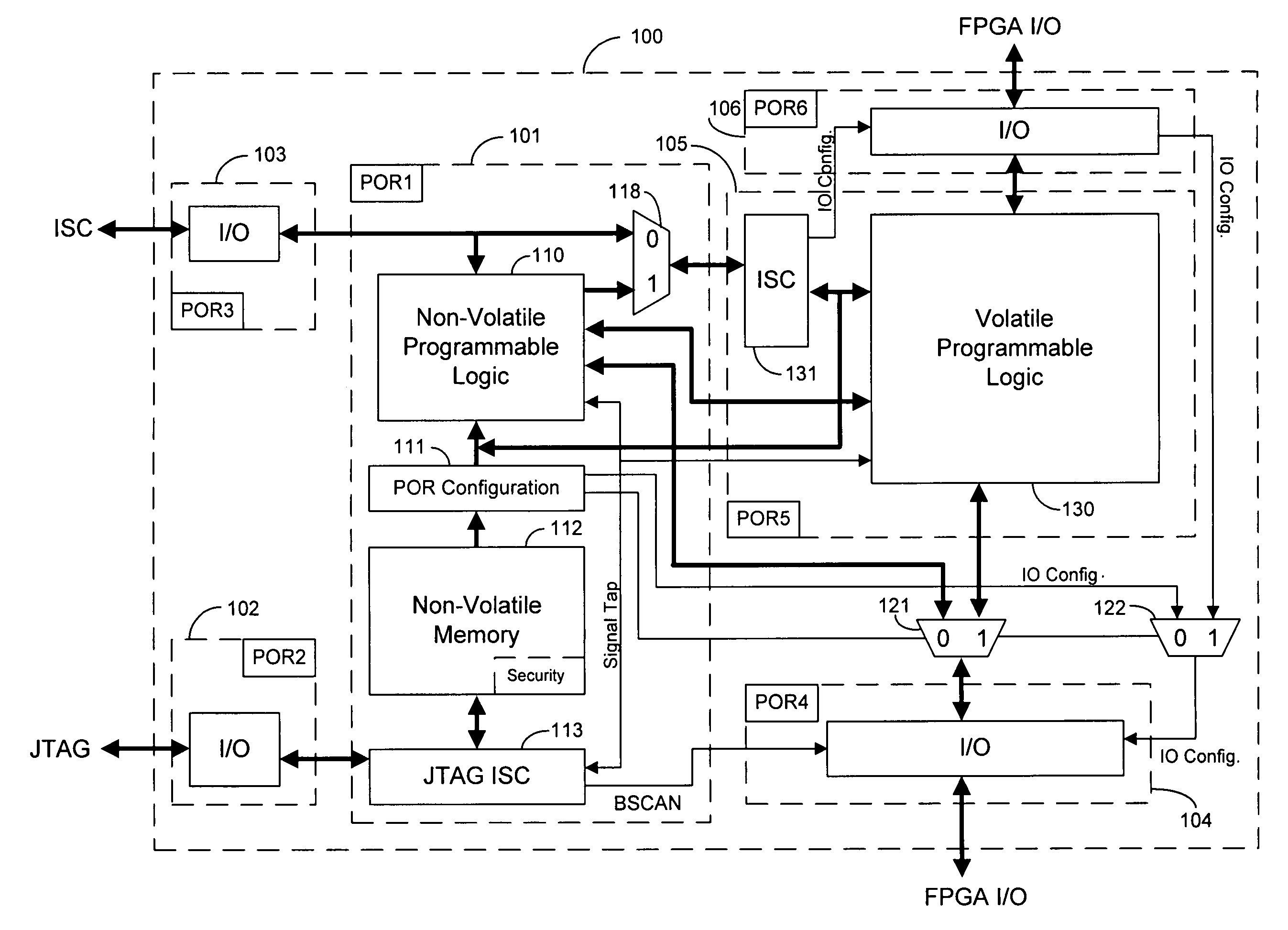
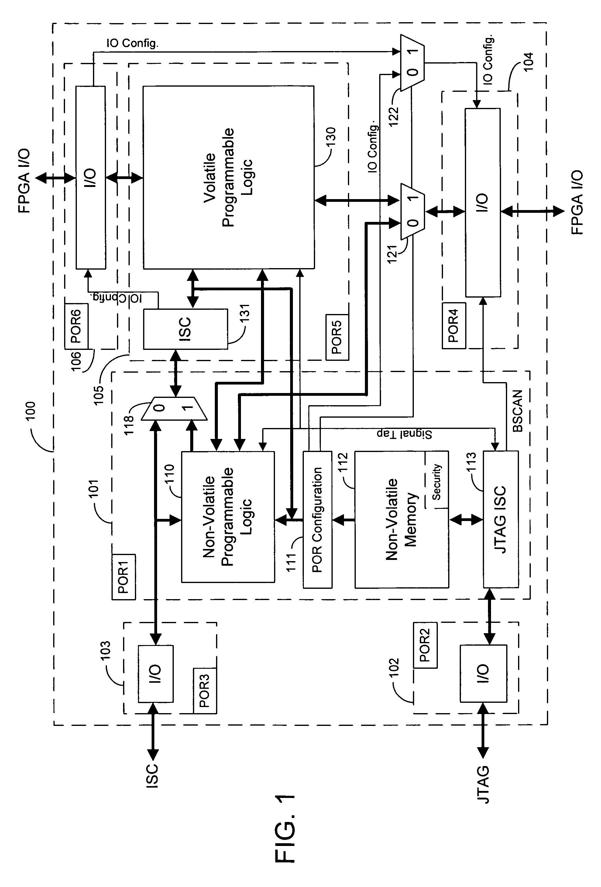
[0015]FIG. 1 illustrates a portion 100 of a programmable logic integrated circuit (IC) that has been designed according to the present invention. Portion 100 includes a first block 110 of programmable logic and a second block 130 of programmable logic. Both programmable logic blocks 110 and 130 contain programmable logic circuits. The programmable logic circuits can be, for example, lookup table based or product term based logic elements. The architecture of the programmable logic arrays in blocks 110 and 130 can be the same or different. Logic blocks 110 and 130 can also include memory. The memory in both of blocks 110 and 130 can be, for example, volatile memory such as SRAM cells.

[0016]The programmable logic in block 110 is configured by configuration bits stored in non-volatile memory block 112. Configuration bits can be stored in non-volatile memory block 112 by a manufacturer or by a user. Power on reset (POR) configuration block 111 transfers configuration bits from non-volat...

second embodiment

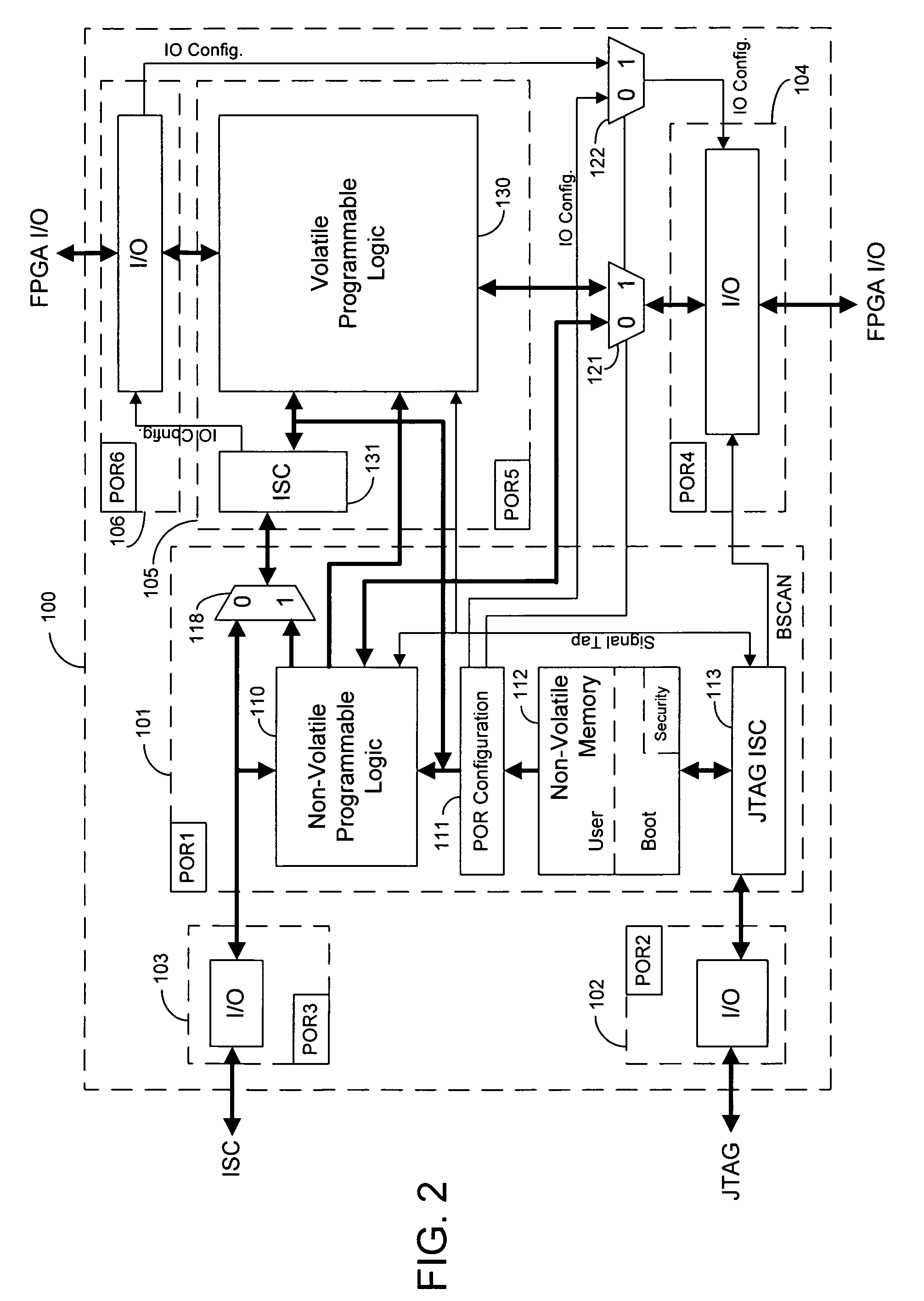
[0040]FIG. 2 illustrates the present invention. According to this embodiment, two sets of configuration data can be stored in memory block 112. The first set of configuration data is a boot pattern that is programmed by the manufacturer to give the FPGA standard functionality for every customer, such as an ASSP. This embodiment has the advantage of allowed a FPGA manufacturer to change the product definition over time by a simple change to out manufacturing test flow.

[0041]Once a user has defined an application, the user can write additional configuration data into memory 112. For example, a user can store configuration data in memory 112 that is used to operate the FPGA in a diagnostic mode to test various signals.

[0042]In an OTP type non-volatile memory, two partitions are need in memory block 112. One partition is used to store the manufacturer's default boot configuration data, and one partition is used to store user configuration data to better meet a user's specific needs. The...


PUM


Abstract

Techniques for combining volatile and non-volatile programmable logic into one integrated circuit (IC) are provided. An IC is segregated into two portions. A first block of programmable logic is configured by bits stored in on-chip non-volatile memory. A second block of programmable logic is configured by bits stored in off-chip memory. The function of IO banks on the IC is multiplexed between the two logic blocks of the IC. The programmable logic in the first block can be configured and fully functional in a fraction of the time that the programmable logic in the second block can be configured. The programmable logic in the first block can configure fast enough and have enough independence to assist in the configuration of the second block. The non-volatile memory can also provide security features to a user design, such as encryption.

Description

BACKGROUND OF THE INVENTION[0001]The present invention provides techniques for combining volatile and non-volatile programmable logic on an integrated circuit (IC), and more particularly, to techniques for providing an IC that has one section of programmable logic configured by off-chip memory and another section of programmable logic configured by on-chip non-volatile memory.[0002]Large field programmable gate arrays (FPGAs) that contain on-chip volatile memory blocks usually require a considerable amount of time to be configured at power-up, because configuration data is loaded onto the chip from an external memory chip. The external memory chip can be, for example, a serial read only memory (SROM).[0003]Small complex programmable logic device (CPLDs) such as Altera's MAX family of CPLDs contain on-chip non-volatile memory. The configuration data is stored in the on-chip non-volatile memory. The configuration data can be loaded quickly from the on-chip non-volatile memory into the...

Claims


Application Information

Patent Timeline
Patent Type & Authority Patents(United States)
IPC IPC(8): H03K19/173G06F7/38H01L25/00H03K19/177
CPCG06F15/7867H03K19/17732H03K19/1776H03K19/17768H03K19/17772H03K19/17776H03K19/17758
Inventor CAMAROTA, RAFAELRAHIM, IRFANANG, BOON JINCHONG, THOW PANG
Owner ALTERA CORP
Why Eureka
Try Eureka