Column-parallel sigma-delta analog-to-digital conversion with gain and offset control

a digital converter and gain control technology, applied in the field of column-parallel sigma-delta analog-to-digital converters, can solve problems such as noise and adverse effects on voltages

Active Publication Date: 2007-07-10
APTINA IMAGING CORP
View PDF11 Cites 28 Cited by
  • Summary
  • Abstract
  • Description
  • Claims
  • Application Information

AI Technical Summary

Problems solved by technology

These voltages, however, may have been adversely impacted by noise during the readout and/or sample and hold operations, which is stored in the Vrst and Vsig...

Method used


Image

  • Column-parallel sigma-delta analog-to-digital conversion with gain and offset control
  • Column-parallel sigma-delta analog-to-digital conversion with gain and offset control
  • Column-parallel sigma-delta analog-to-digital conversion with gain and offset control

Examples


Embodiment Construction

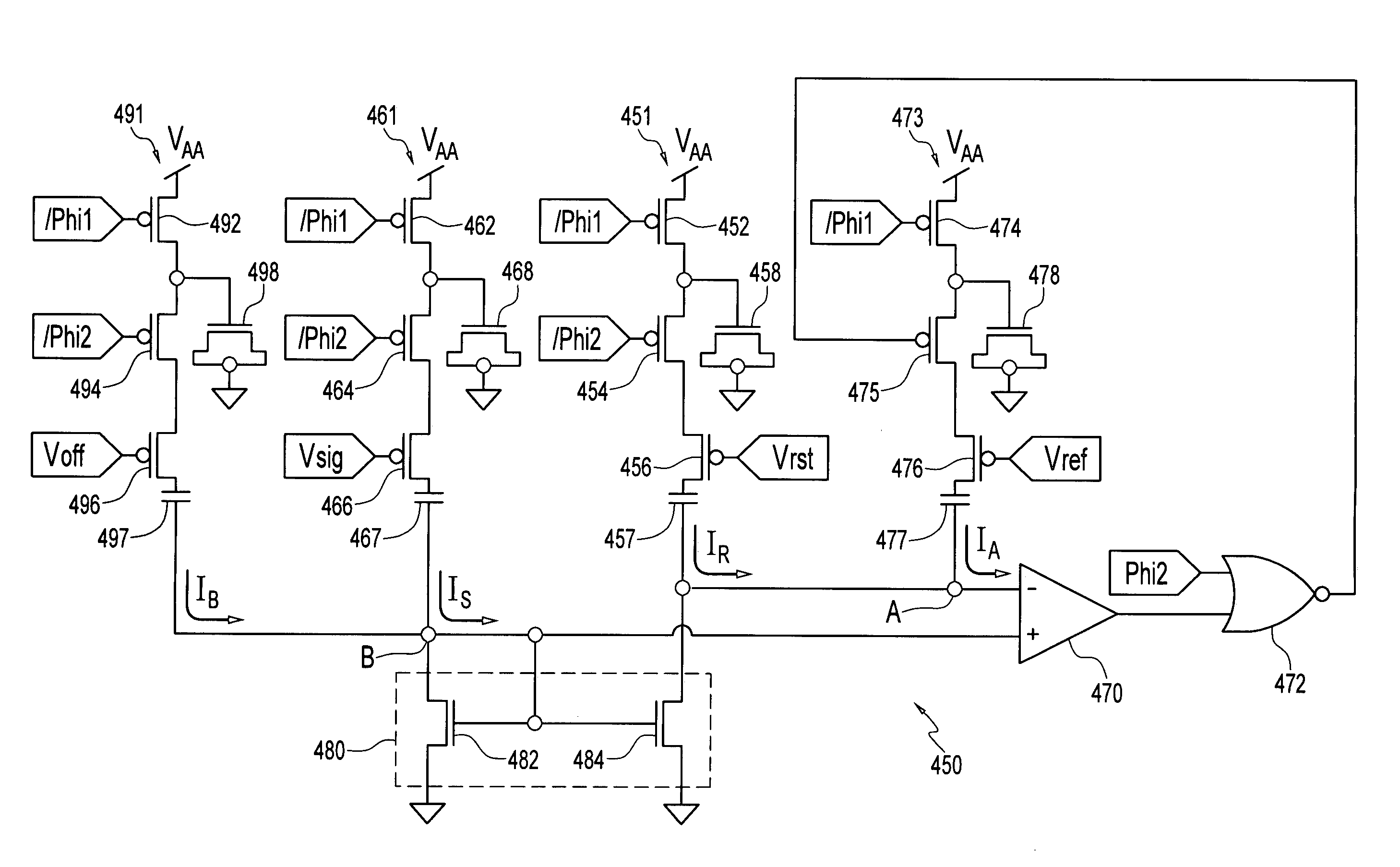
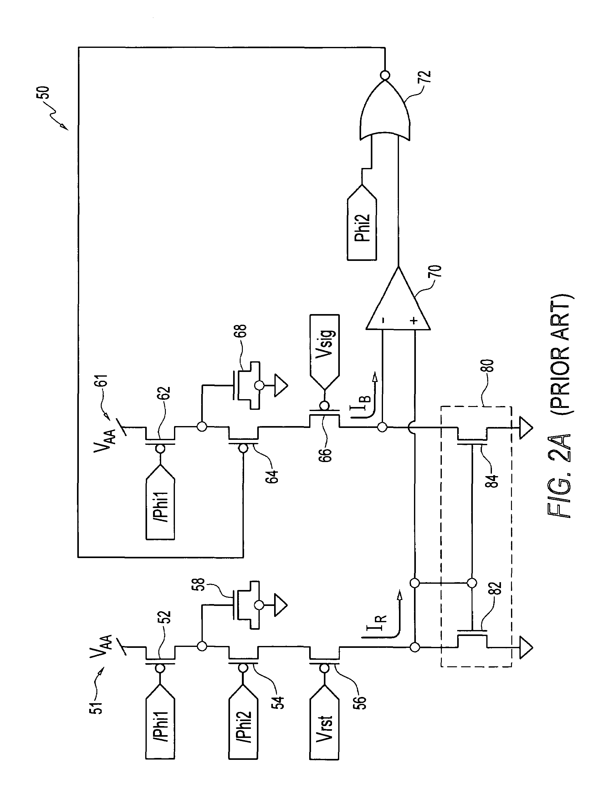
[0028]One method of improving upon the conventional sensing circuit sigma-delta analog-to-digital converter of FIGS. 2A and 2B is presented in U.S. patent application Ser. No. 11 / 106,465, filed Apr. 15, 2005. The '465 method is also demonstrated in FIGS. 3A and 3B. FIG. 3A depicts a sensing circuit 250 and FIG. 3B depicts a sigma-delta analog-to-digital converter 300 that includes sensing circuit 250. The sensing circuit 250 comprises a first branch 251 for sensing the reset signal Vrst from a sample and hold capacitor (not shown), a second branch 261 for sensing the pixel signal Vsig from another sample and hold capacitor (not shown) and a regulation branch 273. The sensing circuit 250 also comprises a current mirror 280, a comparator 270 and a NOR gate 272. The comparator 270 is preferably a regenerative latch type comparator, where the digital output is synchronized to the phase clocks.

[0029]The first branch 251 comprises three PMOS transistors 252, 254, 256 and a capacitor 258. ...


PUM


Abstract

A sigma-delta modulation sensing circuit and an analog-to-digital converter for an imager that eliminate the erroneous conversion of non-zero analog voltages to zero digital voltages is provided. The sensing circuit includes an offset branch that allows input of an offset voltage that is at least as large as a negative channel-specific offset found in a pixel signal voltage. The sensing circuit also includes a regulation branch based on a reference voltage common across multiple columns of an imager. The regulation branch has an adjustable resistance that is modulated during the sensing operation, which creates an adjustment current that is applied during the sensing operation to a reset signal. The sensing circuit and analog-to-digital converter generate digital code based on the difference between the reset voltage and the summed offset and pixel signal voltage.

Description

FIELD OF THE INVENTION[0001]The invention relates generally to a sigma-delta analog-to-digital converter and more particularly to a sigma-delta analog-to-digital converter used in imaging devices.BACKGROUND OF THE INVENTION[0002]Semiconductor imagers are used in a variety of digital image capture systems, including products such as scanners, copiers, and digital cameras. A semiconductor imager typically includes an array of light-sensitive pixel cells that are electrically responsive to incident light. Each cell in a pixel cell array includes a photosensor for converting incident photons into charge. The collected charge in each cell is output as a pixel signal voltage. The collective pixel signal voltages are processed to generate a digital version of the captured image.[0003]FIG. 1 illustrates a block diagram of an exemplary semiconductor CMOS imager 100 having a pixel array 140 comprising a plurality of pixel cells arranged in a predetermined number of columns and rows. Each pixe...

Claims


Application Information

Patent Timeline
IPC IPC(8): H03M1/06
CPCH03M1/0604H03M1/123
Inventor BOEMLER, CHRISTIAN
Owner APTINA IMAGING CORP
Why Eureka
Try Eureka