Method of fabricating a field effect transistor having improved junctions

a field effect transistor and junction technology, applied in the direction of transistors, semiconductor devices, electrical equipment, etc., can solve the problems of high external resistance, unacceptably high leakage current and/or high external resistance, and conventional methods of annealing by which an implanted substrate is heated to drive the diffusion of dopants

Inactive Publication Date: 2007-07-24
GOOGLE LLC
View PDF13 Cites 56 Cited by
  • Summary
  • Abstract
  • Description
  • Claims
  • Application Information

AI Technical Summary

Problems solved by technology

Conventional methods of annealing by which an implanted substrate is heated to drive the diffusion of dopants do not produce sufficiently abrupt and small junction depth because the dopants move too far under such heating.
However, when the substrate is not heated long enough, dislocations in the crystal structure of the semiconductor remain at the boundary between an implanted region of the crystalline semiconductor and unimplanted regions.
These dislocations lead to problems, such as unacceptably high leakage current and / or high external resistance.

Method used


Image

  • Method of fabricating a field effect transistor having improved junctions
  • Method of fabricating a field effect transistor having improved junctions
  • Method of fabricating a field effect transistor having improved junctions

Examples


Embodiment Construction

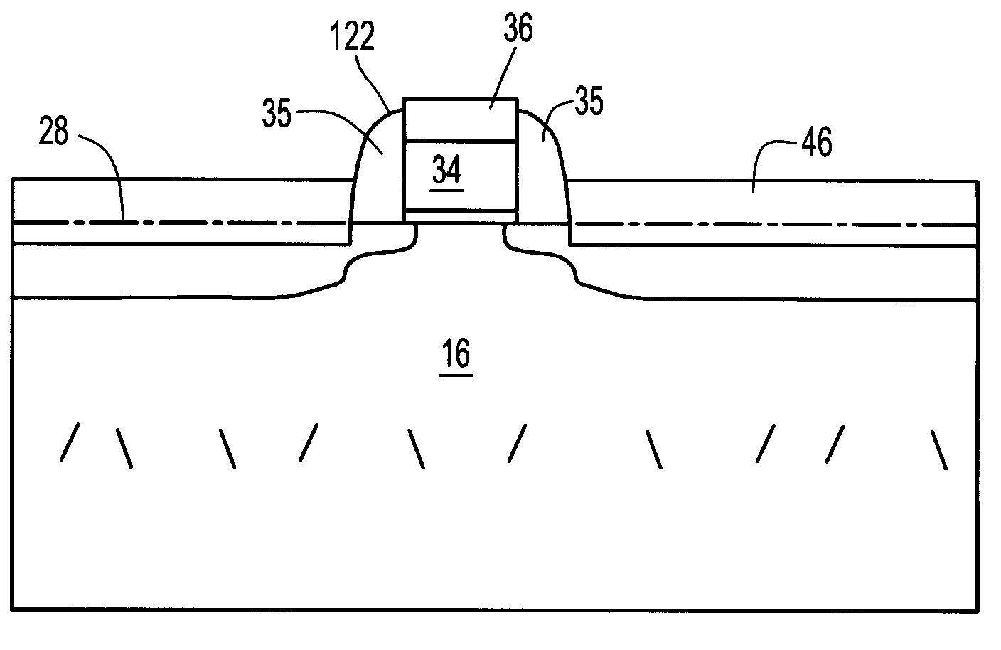
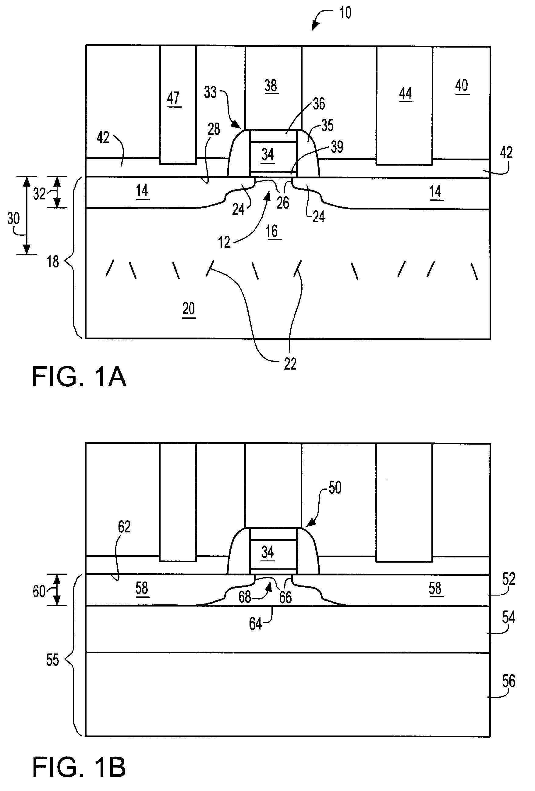
[0007]FIG. 1A illustrates a field effect transistor (FET) 10 according to an embodiment of the invention. As shown therein, the FET includes a channel region 12 in a first single-crystal region 16 of a substrate and a pair of source / drain regions 14 flanking the channel region 12 in portions of the single-crystal region 16 adjacent to the channel region 12. The invention will be described first with reference to an embodiment in which the single-crystal region 16 is disposed within a bulk substrate 18. Then, the necessary modifications will be described for an embodiment in which the single-crystal region 16 forms the active device layer of a semiconductor-on-insulator (SOI) substrate.

[0008]As shown in FIG. 1A, defects, e.g., dislocations 22 in the crystal structure define a boundary between the first single-crystal region 16 in which the channel region 12 and the source / drain regions 14 are disposed, and a lower single-crystal portion 20 of the substrate 18 below the first single-c...


PUM


Abstract

A method of forming a field effect transistor is provided which includes forming an amorphized semiconductor region having a first depth from a single-crystal semiconductor region and subsequently forming a first gate conductor above a channel portion of the amorphized semiconductor region. A first dopant including at least one of an n-type dopant and a p-type dopant is then implanted to a second depth into portions of the amorphized semiconductor region not masked by the first gate conductor to form source / drain portions adjacent to the channel portion. The substrate is then heated to recrystallize the channel portion and the source / drain portions of the amorphized semiconductor region. After the heating step, at least a part of the recrystallized semiconductor region is locally heated to activate a dopant in at least one of the channel portion and the source / drain portion.

Description

BACKGROUND OF THE INVENTION[0001]The present invention relates to active semiconductor devices and their fabrication, and more particularly to a structure and method of fabricating a field effect transistor.[0002]It is highly desirable for field effect transistors having deep sub-micron dimensions (those having conduction channels of width less than about 50 nm) to have very sharp and small junction depth. Conventional methods of annealing by which an implanted substrate is heated to drive the diffusion of dopants do not produce sufficiently abrupt and small junction depth because the dopants move too far under such heating. Methods of laser annealing, by contrast, can produce sufficiently small junction depth. However, when the substrate is not heated long enough, dislocations in the crystal structure of the semiconductor remain at the boundary between an implanted region of the crystalline semiconductor and unimplanted regions. These dislocations lead to problems, such as unaccept...

Claims


Application Information

Patent Timeline
Patent Type & Authority Patents(United States)
IPC IPC(8): H01L21/20H01L21/36
CPCH01L21/26506H01L29/66545H01L29/6659H01L29/7833H01L29/51
Inventor ZHU, HUILONGGLUSCHENKOV, OLEGSUNG, CHUN-YUNG
Owner GOOGLE LLC
Why Eureka
Try Eureka